Semiconductor package with improved chip attachment and manufacturing method thereof

Inactive Publication Date: 2005-02-24
SAMSUNG ELECTRONICS CO LTD
View PDF25 Cites 11 Cited by
  • Summary
  • Abstract
  • Description
  • Claims
  • Application Information

AI Technical Summary

Benefits of technology

[0012] A semiconductor package comprises a chip having a top surface for chip pads and a bottom surface opposite the top surface. The top and bottom surfaces define side surfaces. The package further includes an adhesive layer provided within a chip-attaching area substantially defined by side surfaces of the chip and attaches a chip to, for example, a substrate having substrate pads. This prevents the

Problems solved by technology

This may result in poor bonding of the wires 13 on the substrate pads 12a.
In

Method used


Image

  • Semiconductor package with improved chip attachment and manufacturing method thereof
  • Semiconductor package with improved chip attachment and manufacturing method thereof
  • Semiconductor package with improved chip attachment and manufacturing method thereof

Examples


Embodiment Construction

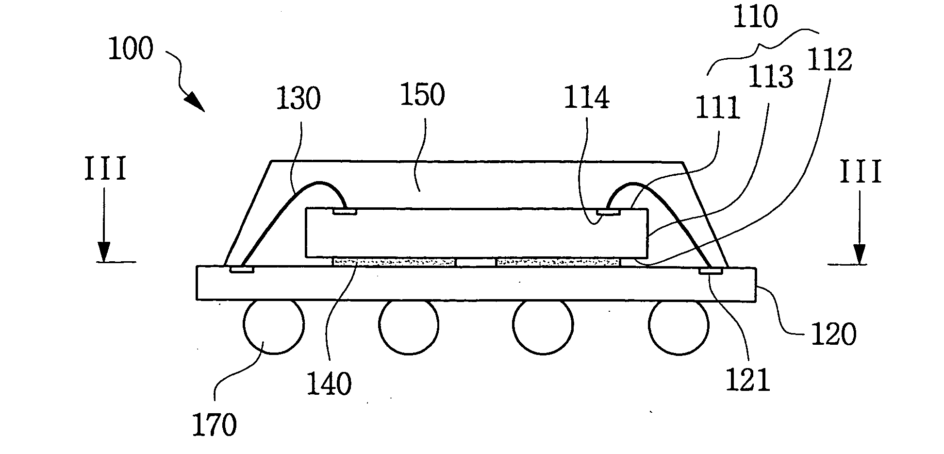
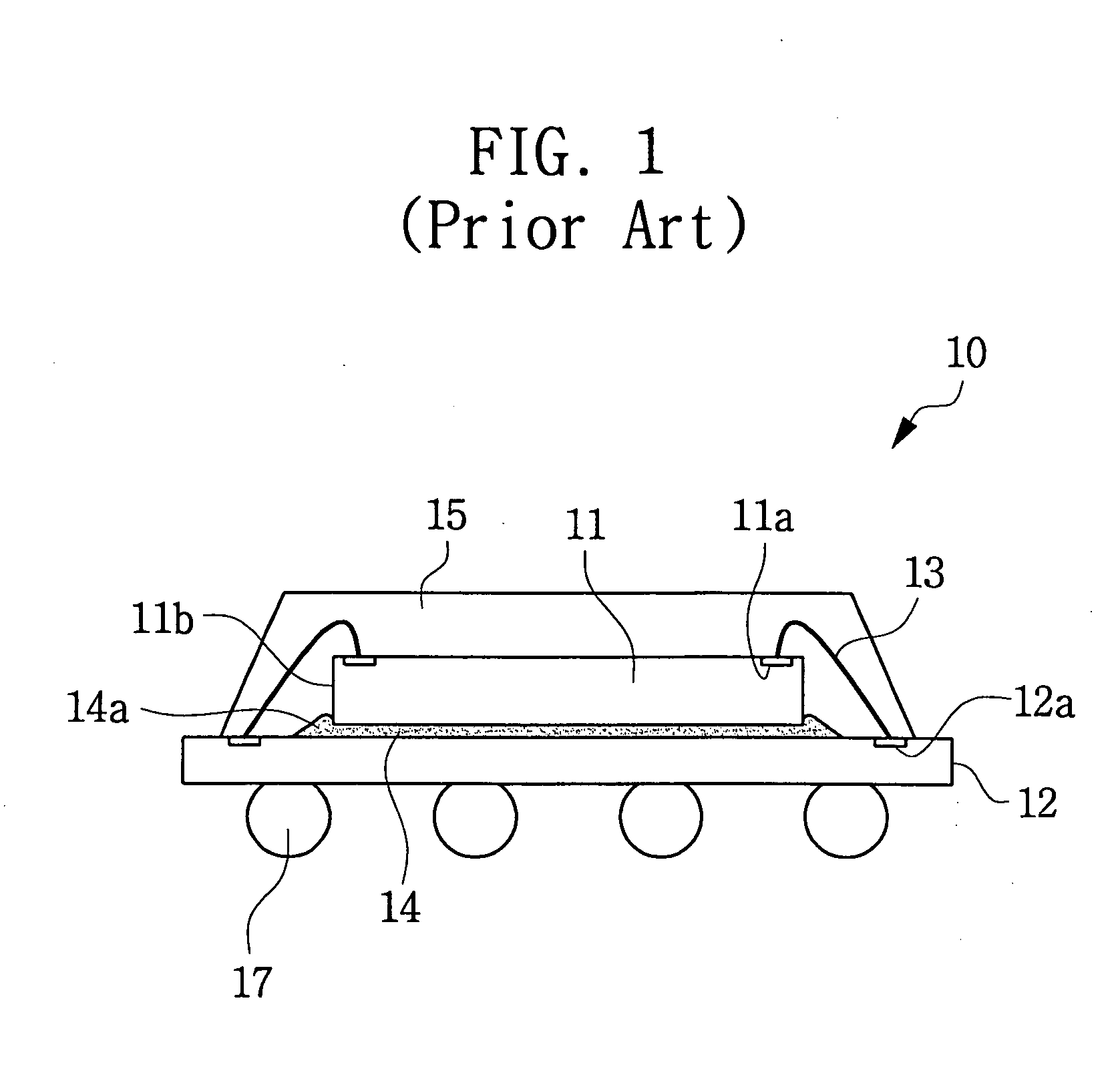
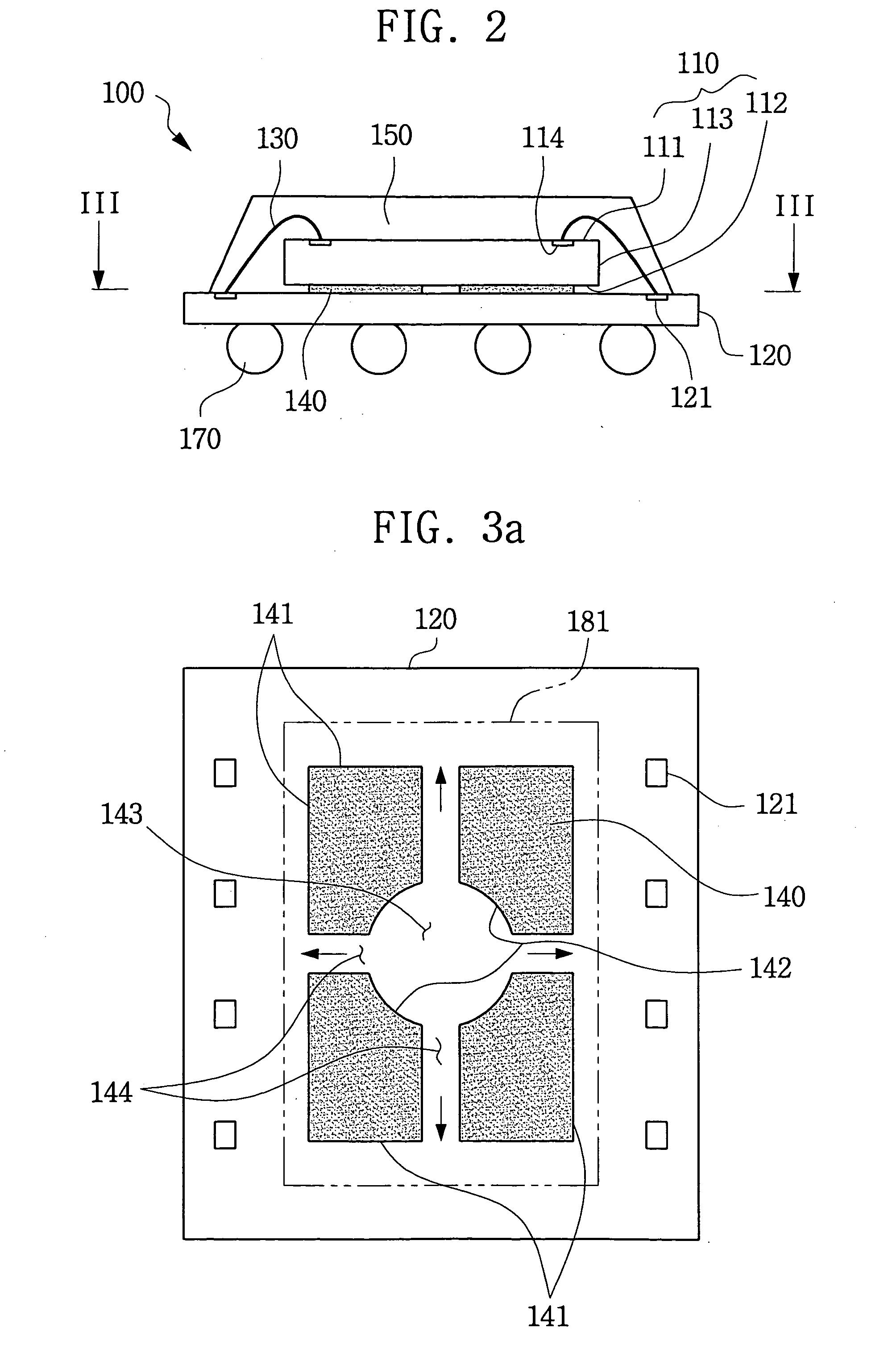
[0022] The present invention will now be described more fully hereinafter with reference to the accompanying drawings, in which several preferred embodiments of the invention are shown. This invention may, however, be embodied in many different forms and is not limited to the embodiments presented in this disclosure. Rather, these embodiments are provided so that this disclosure will be thorough and complete, and will fully convey the scope of the invention to those skilled in the art.

[0023] In the description, well-known structures and processes have not been shown in detail to avoid obscuring the present invention. It will be appreciated that for simplicity and clarity of illustration, some elements illustrated in the figures have not necessarily been drawn to scale. For example, the dimensions of some of the elements are exaggerated relative to other elements for clarity. Like numerals are used for like and corresponding parts of the various drawings.

[0024]FIG. 2 schematically ...


PUM


Abstract

A semiconductor package comprises a chip having a top surface for chip pads and a bottom surface opposite the top surface. The top and bottom surfaces define side surfaces. The package further includes an adhesive layer provided within a chip-attaching area substantially defined by side surfaces of the chip and attaches a chip to, for example, a substrate having substrate pads. This prevents the contamination of the substrate pads by the adhesive layer. In one embodiment, the adhesive layer has at least one hole formed therethrough to expose a portion of the bottom surface of the chip. The adhesive layer may include at least one passage laterally connecting the hole to the outside. Alternatively, the adhesive layer has a plurality of adhesive parts separately disposed on the semiconductor chip.

Description

CROSS REFERENCE TO RELATED APPLICATIONS [0001] This U.S. non-provisional application claims priority under 35 U.S.C. §119 to Korean Patent Application No. 2003-58274 filed Aug. 22, 2003, the contents of which are incorporated by reference. BACKGROUND OF THE INVENTION [0002] 1. Field of the Invention [0003] The present invention relates generally to electronic packaging technology and, more particularly, to semiconductor packages having improved chip-attaching structures and methods for manufacturing the semiconductor packages with improved chip-attaching reliability. [0004] 2. Description of the Related Art [0005] In general, an electronic package or a semiconductor package is defined as the housing and interconnection of integrated circuits (also referred to as ‘semiconductor chips’, ‘chips’, or ‘die’) to form an electronic system. The functions which the package must provide include a structure to physically support the chip, a physical housing to protect the chip from the environ...

Claims


Application Information

Patent Timeline
IPC IPC(8): H01L23/52H01L21/58H01L23/02H01L23/498
CPCH01L23/49816H01L2924/0665H01L24/32H01L24/743H01L24/83H01L2224/32014H01L2224/32145H01L2224/32225H01L2224/48091H01L2224/48227H01L2224/73265H01L2224/743H01L2224/83194H01L2224/8385H01L2224/8592H01L2224/92247H01L2225/0651H01L2225/06575H01L2924/07802H01L2924/14H01L2924/15311H01L24/27H01L2924/014H01L2924/01033H01L2924/01023H01L2924/01006H01L2224/2919H01L2924/00014H01L2924/00H01L2924/00012H01L2924/181H01L24/73H01L23/52
Inventor LEE, JONG-UNGSIN, WHA-SUJEON, JONG-KEUN
Owner SAMSUNG ELECTRONICS CO LTD
Why Eureka
Try Eureka