Polishing pad having a sealed pressure relief channel

Inactive Publication Date: 2007-02-15
KUO CHARLES C +1
View PDF3 Cites 8 Cited by
  • Summary
  • Abstract
  • Description
  • Claims
  • Application Information

AI Technical Summary

Benefits of technology

[0008] Hence, what is needed is a polishing pad having a reduced stress window for robust end-point detection or measurement during CMP over a wide range of wavelengths.
[0009] In a first aspect of the present invention, there is provided a chemical mechanical polishing pad comprising: a window formed in the polishing pad, the window having a void provided on a side thereof; a pressure relief channel provided in the polishing pad from the void to a periphery of the polishing pad; and a membrane provided in the channel to prevent contamination of the void.
[0010] In another aspect of the present invention, there is provided a chemical mechanical polishing pad comprising: a polishing layer having a window formed therein, the window being exposed to a void on

Problems solved by technology

Unfortunately, during polishing, undue stress is applied to the window from the pressure that is generated in the void and may cause unwanted residual stress deformations

Method used


Image

  • Polishing pad having a sealed pressure relief channel
  • Polishing pad having a sealed pressure relief channel
  • Polishing pad having a sealed pressure relief channel

Examples


Example

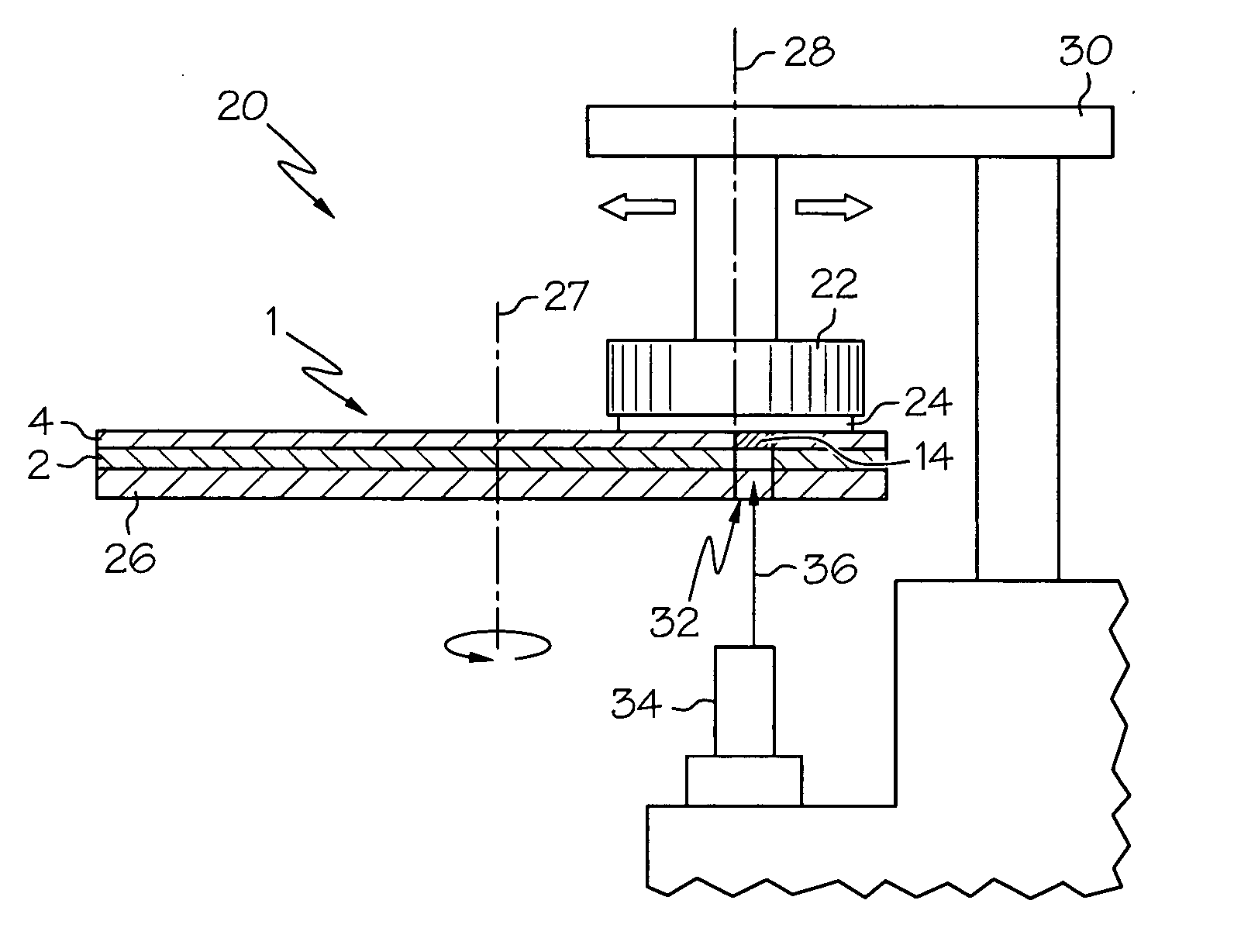
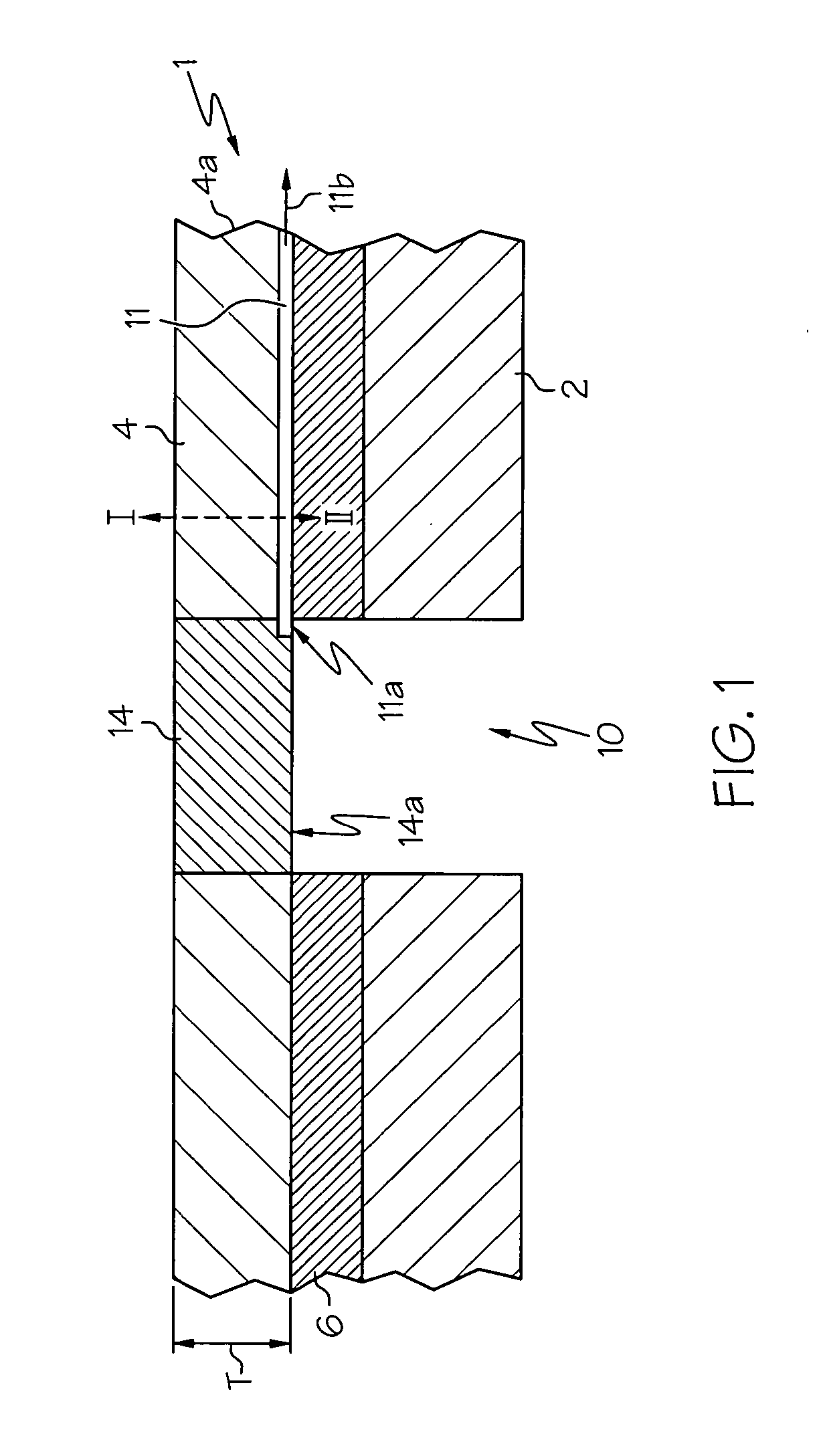
[0019] Referring now to FIG. 1, a polishing pad 1 of the present invention is shown. Polishing pad 1 comprises a polishing layer 4 and an optional bottom layer 2. Note, polishing layer 4 and bottom layer 2 may individually serve as a polishing pad. In other words, the present invention may be utilized in the polishing layer 4 alone, or in the polishing layer 4 in conjunction with the bottom layer 2, as a polishing pad. The bottom layer 2 may be made of felted polyurethane, such as SUBA-IV™ pad manufactured by Rohm and Haas Electronic Materials CMP Inc. (“RHEM”), of Newark, Del. The polishing layer 4 may comprise a polyurethane pad (e.g., a pad filled with microspheres), such as, IC 1000™ pad by RHEM. Polishing layer 4 may optionally be texturized as desired. A thin layer of pressure sensitive adhesive 6 may hold the polishing layer 4 and the bottom layer 2 together. The adhesive 6 may be commercially available from 3M Innovative Properties Company of St, Paul, Minn.

[0020] Polishing...


PUM


Abstract

The present invention provides a chemical mechanical polishing pad comprising a window formed in the polishing pad, the window having a void provided on a side thereof. The invention further provides a pressure relief channel provided in the polishing pad from the void to a periphery of the polishing pad. In addition, a membrane is provided in the channel to prevent contamination of the void.

Description

CROSS REFERENCE TO RELATED APPLICATION [0001] This application claims the benefit of U.S. Provisional Application Ser. No. 60 / 706,873 filed Aug. 10, 2005.BACKGROUND OF THE INVENTION [0002] The present invention relates to polishing pads for chemical mechanical planarization (CMP), and in particular, relates to polishing pads having reduced stress windows formed therein for performing optical end-point detection. Further, the present invention relates to polishing pads having a sealed pressure relief channel to reduce stress on the windows and prevent contamination of the window area. [0003] In the fabrication of integrated circuits and other electronic devices, multiple layers of conducting, semiconducting and dielectric materials are deposited on or removed from a surface of a semiconductor wafer. Thin layers of conducting, semiconducting, and dielectric materials may be deposited by a number of deposition techniques. Common deposition techniques in modem processing include physica...

Claims


Application Information

Patent Timeline
IPC IPC(8): B24B49/00B24D11/00
CPCB24B37/205
Inventor KUO, CHARLES C.O'SULLIVAN, JENNIFER M.
Owner KUO CHARLES C
Why Eureka
Try Eureka