Semiconductor device and method of manufacturing the same, circuit board, and electronic instrument

a semiconductor and chip technology, applied in the direction of semiconductor devices, semiconductor/solid-state device details, electrical devices, etc., can solve problems such as warping or cracks in one of the semiconductor chips

Active Publication Date: 2005-03-10
ADVANCED INTERCONNECT SYST LTD
View PDF4 Cites 153 Cited by
  • Summary
  • Abstract
  • Description
  • Claims
  • Application Information

AI Technical Summary

Problems solved by technology

However, warping or cracks may occur in one of the semicon...

Method used


Image

  • Semiconductor device and method of manufacturing the same, circuit board, and electronic instrument
  • Semiconductor device and method of manufacturing the same, circuit board, and electronic instrument
  • Semiconductor device and method of manufacturing the same, circuit board, and electronic instrument

Examples


Embodiment Construction

[0029] An objective of the present invention is to improve reliability of a semiconductor device and a method of manufacturing the same, a circuit board, and an electronic instrument.

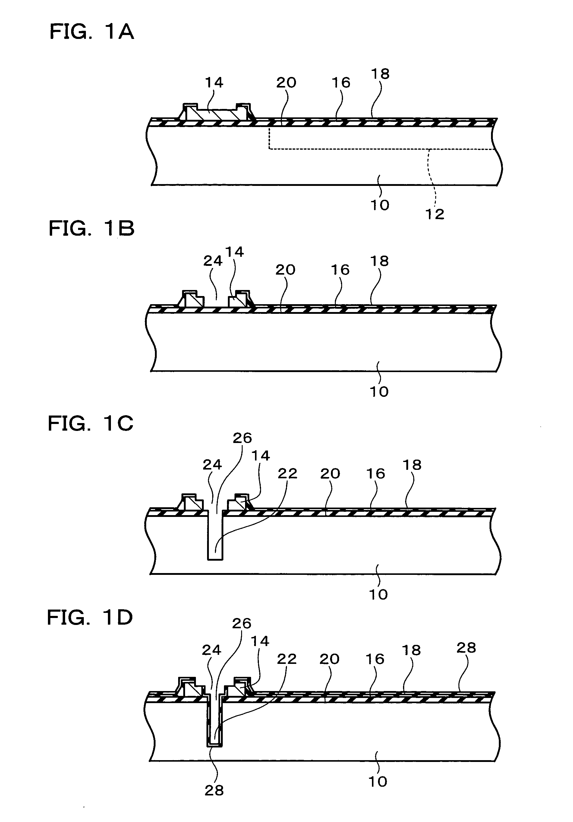
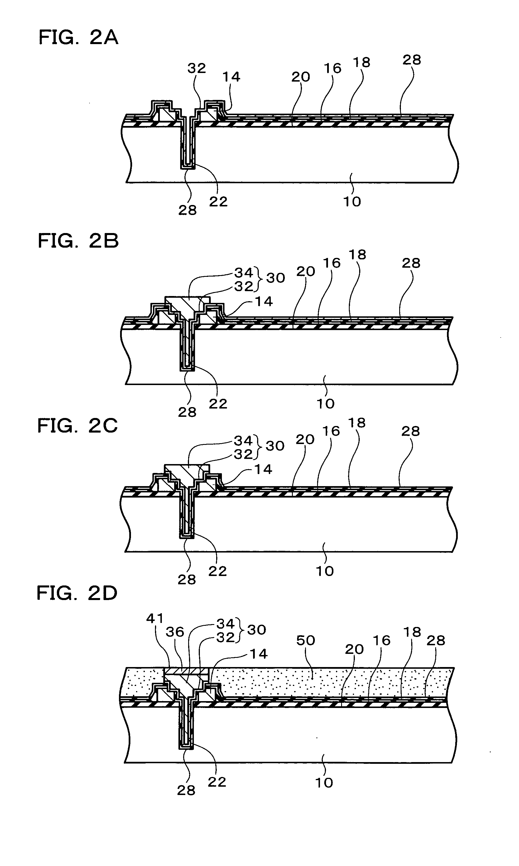
[0030] (1) According to one embodiment of the present invention, there is provided a method of manufacturing a semiconductor device, comprising: [0031] (a) forming a first resin layer on a first surface of a semiconductor substrate, an integrated circuit being formed in the first surface of the semiconductor substrate; [0032] (b) forming a through-hole electrode including a second projecting section which projects from a second surface opposite to the first surface by removing a part of the semiconductor substrate from the second surface so as to thin the semiconductor substrate; and [0033] (c) forming a second resin layer on the second surface of the semiconductor substrate with at least a part of a surface of the second projecting section being exposed.

[0034] According to this embodiment, the resin ...


PUM


Abstract

A method of manufacturing a semiconductor device includes: (a) forming a first resin layer on a first surface of a semiconductor substrate, an integrated circuit being formed in the first surface of the semiconductor substrate; (b) forming a through-hole electrode including a projecting section which projects from a second surface opposite to the first surface by removing a part of the semiconductor substrate from the second surface so as to thin the semiconductor substrate; and (c) forming a second resin layer on the second surface of the semiconductor substrate so as to avoid the projecting section.

Description

[0001] Japanese Patent Application No. 2003-175323, filed on Jun. 19, 2003, is hereby incorporated by reference in its entirety. BACKGROUND OF THE INVENTION [0002] The present invention relates to a semiconductor device and a method of manufacturing the same, a circuit board, and an electronic instrument. [0003] A semiconductor device in three-dimensional mounting form has been developed. It is known in the art that through-hole electrodes are formed in semiconductor chips, and the upper and lower through-hole electrodes are bonded by stacking the semiconductor chips. The space between the stacked semiconductor chips is filled with a resin (underfill material). However, warping or cracks may occur in one of the semiconductor chips due to stress caused by cure shrinkage of the resin. In particular, since the resin is provided on only one side (lower side) of the uppermost semiconductor chip, stress caused by cure shrinkage of the resin is applied from one side, whereby warping or cra...

Claims


Application Information

Patent Timeline
IPC IPC(8): H01L23/52H01L21/00H01L21/301H01L21/3205H01L21/768H01L23/02H01L25/065H01L25/07H01L25/18
CPCH01L21/76898H01L25/50H01L2224/16145H01L2225/06513H01L2225/06541H01L2224/16146H01L2924/15311H01L2924/3025H01L2224/13009H01L2224/14181H01L2924/01078H01L24/05H01L2224/05001H01L2224/05009H01L2224/05025H01L2224/05124H01L2224/05556H01L2224/13025H01L2924/00014
Inventor FUKAZAWA, MOTOHIKO
Owner ADVANCED INTERCONNECT SYST LTD
Why Eureka
Try Eureka