Supercharge Your Innovation With Domain-Expert AI Agents!

Lead frame with flag support structure

a technology of flag support and lead frame, which is applied in the direction of semiconductor devices, semiconductor/solid-state device details, electrical apparatus, etc., can solve the problems of stress on the packaging die during manufacture and operating conditions, affecting the operation of the device, and complicated stress isolation process

Inactive Publication Date: 2005-03-17
NORTH STAR INNOVATIONS
View PDF8 Cites 10 Cited by
  • Summary
  • Abstract
  • Description
  • Claims
  • Application Information

AI Technical Summary

Problems solved by technology

Because the packaging of die includes different materials (e.g. metal, encapsulant), temperature variations may cause the packaged die to be stressed during manufacture and operating conditions due to the differences in thermal expansion and other material properties of the different materials.
For some packaged electronic devices that include some types of circuits and transducers (e.g. a sensor), this stress may affect the operation of the device.
Such a stress isolation process is complicated and the process control is often difficult.

Method used


Image

  • Lead frame with flag support structure
  • Lead frame with flag support structure
  • Lead frame with flag support structure

Examples


Embodiment Construction

[0016] The following sets forth a detailed description of a mode for carrying out the invention. The description is intended to be illustrative of the invention and should not be taken to be limiting.

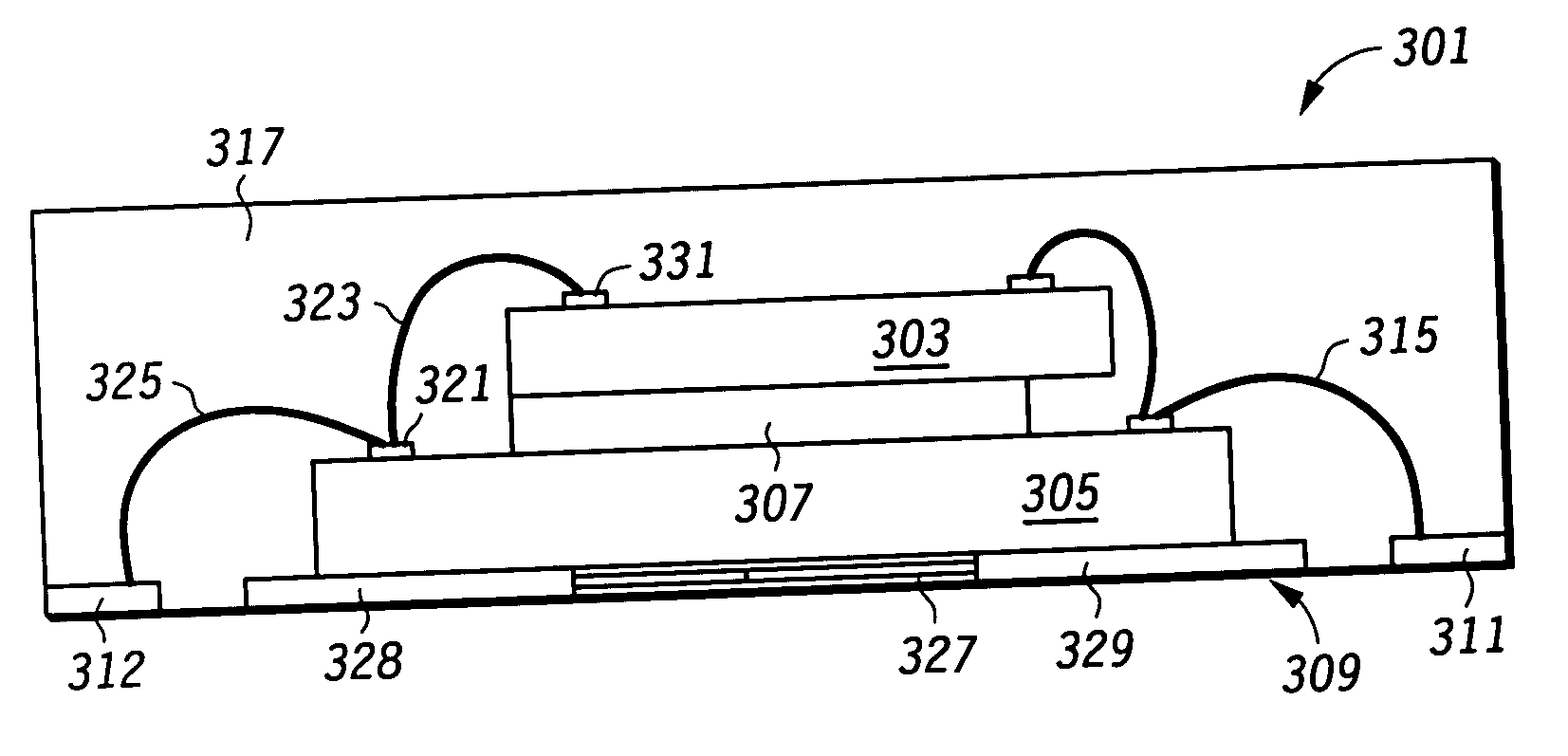
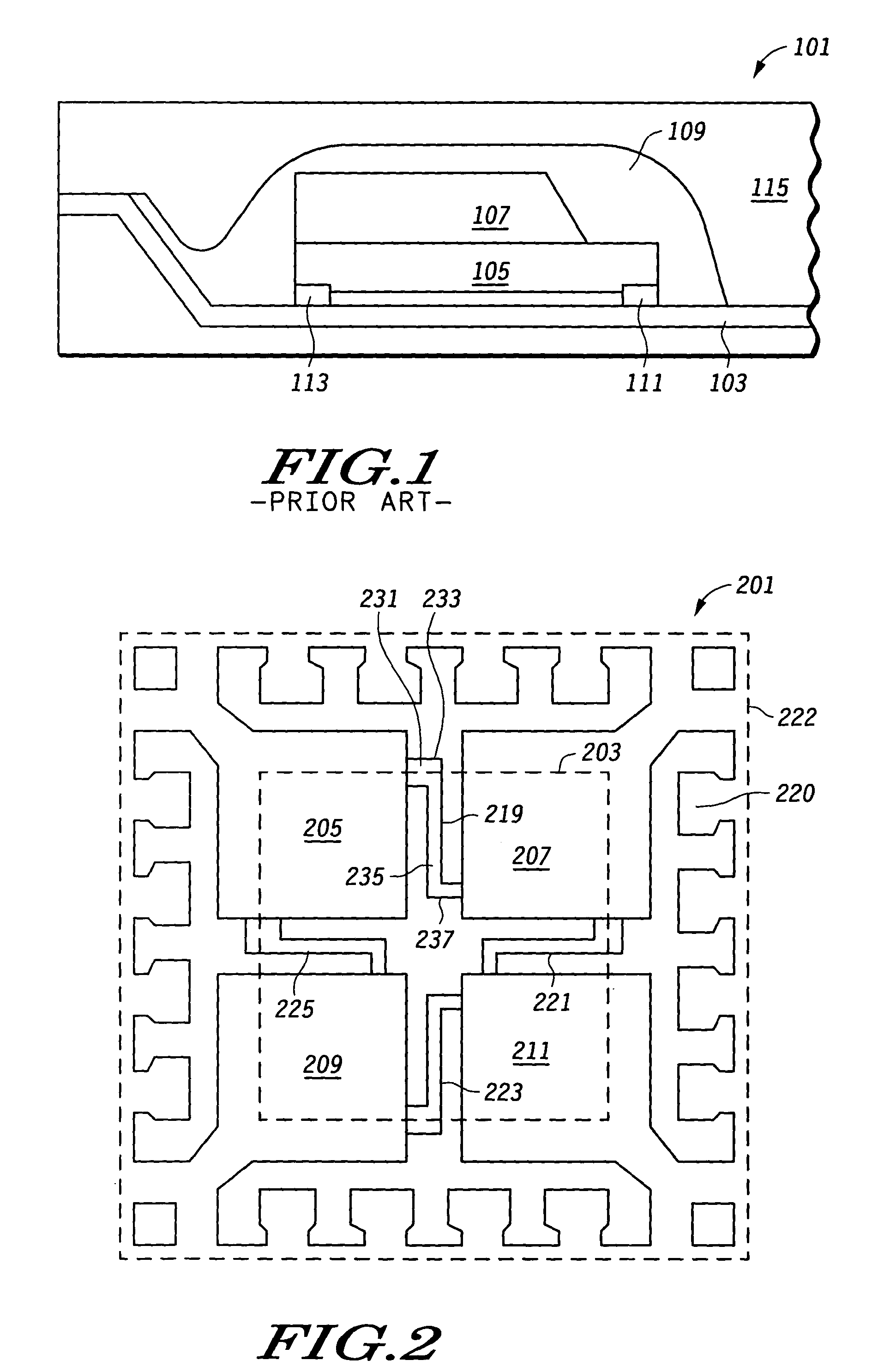
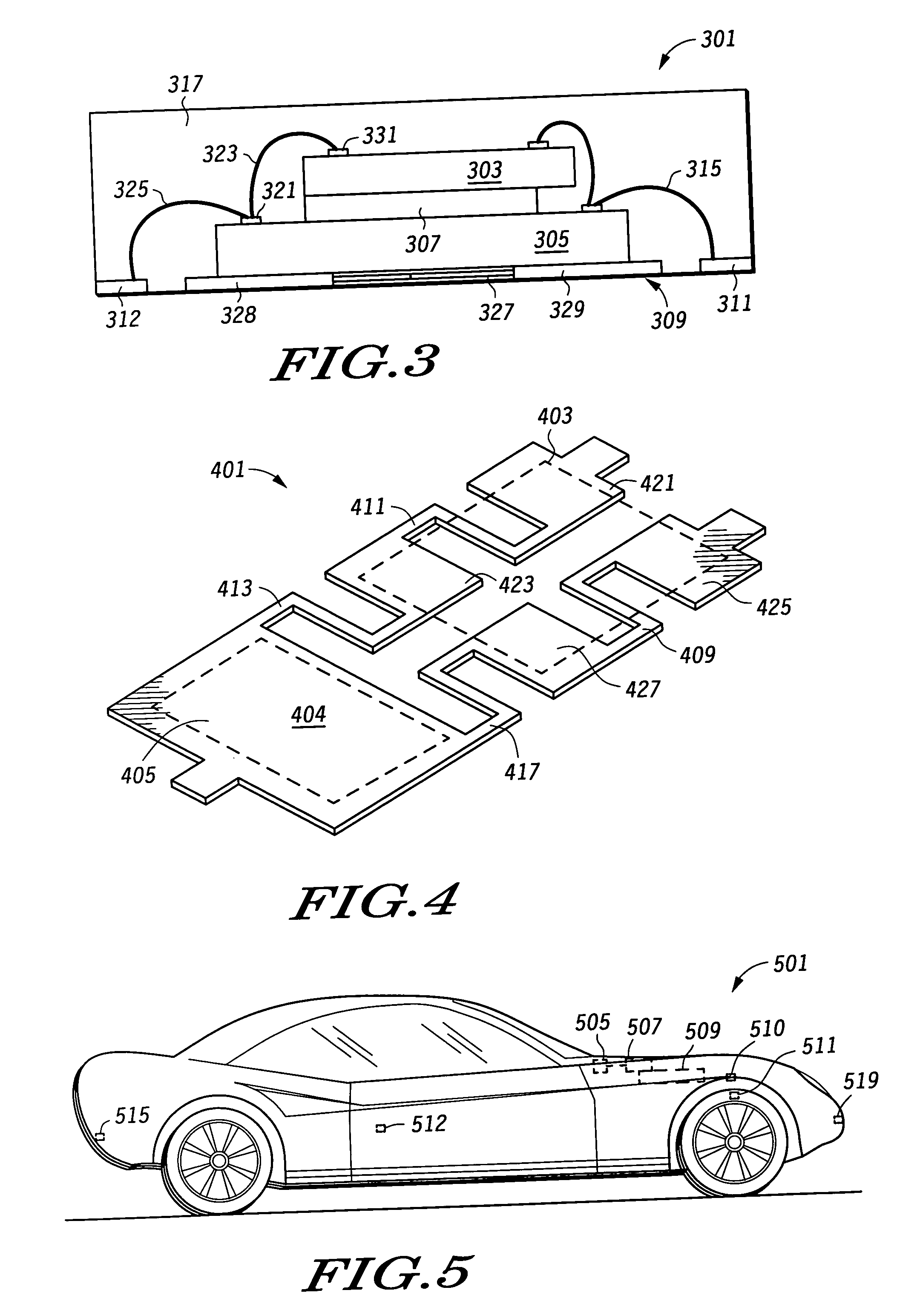
[0017]FIG. 2 shows a top view of a lead frame for a packaged electronic device according to the present invention. Lead frame 201 includes a die mounting location 203 located on its top side (relative to the view shown in FIG. 2). Die mounting location 203 defines the location of a die with respect to a lead frame in a packaged electronic device. Lead frame 201 includes four split flag structures 205, 207, 209, and 211. The top side of each flag structure includes a portion of die mounting location 203.

[0018] In the embodiment shown, lead frame 201 also includes wire bond pads (e.g. 220) where wires (not shown) are bonded for coupling to the bond pads (not shown) of the die via bond wires (e.g. 315 of FIG. 3). After encapsulating lead frame 201 and die, portions (e.g. 222) of lead fra...


PUM


Abstract

A lead frame (201) for a packaged electronic device having split flag structures (205, 207) coupled by support structures (219). The support structures include bend portions (233) for providing stress relief between the flag structures during the manufacture and / or during the operation of a packaged electronic device (301). In one embodiment, the packaged electronic device includes an inertial sensor (515).

Description

BACKGROUND OF THE INVENTION [0001] 1. Field of the Invention [0002] This invention relates in general to packaged electronic devices and specifically to lead frames for packaged electronic devices. [0003] 2. Description of the Related Art [0004] Electrical circuits such as integrated circuits can be implemented in packaged electronic devices. A packaged electronic device may include one or more lead frames and one or more die for implementing electrical circuits of the packaged electronic device. In some embodiments, the die and lead frame(s) may be encapsulated with an encapsulant. [0005] Because the packaging of die includes different materials (e.g. metal, encapsulant), temperature variations may cause the packaged die to be stressed during manufacture and operating conditions due to the differences in thermal expansion and other material properties of the different materials. For some packaged electronic devices that include some types of circuits and transducers (e.g. a sensor)...

Claims


Application Information

Patent Timeline
IPC IPC(8): H01L23/495
CPCH01L23/49503H01L24/48H01L23/49575H01L2224/32014H01L2224/32145H01L2224/32245H01L2224/48091H01L2224/48145H01L2224/48247H01L2224/73265H01L2924/01029H01L2924/01082H01L2924/14H01L2924/1433H01L2924/3025H01L23/49551H01L24/32H01L2924/00014H01L2924/181H01L2924/00012H01L2224/45099H01L2224/45015H01L2924/207
Inventor LI, GARY G.CHAPMAN, MICHAEL E. S.MAHADEVAN, DAVE S.
Owner NORTH STAR INNOVATIONS
Features
  • R&D
  • Intellectual Property
  • Life Sciences
  • Materials
  • Tech Scout
  • Unparalleled Data Quality
  • Higher Quality Content
  • 60% Fewer Hallucinations
Learn More