Conductive connection structure with stress reduction arrangement for a semiconductor device, and related fabrication method

a technology of conductive connection structure and semiconductor device, which is applied in the direction of semiconductor devices, solid-state devices, basic electric elements, etc., can solve the problems of high stress, high stress, and high stress of low-k and ulk materials typically used in semiconductor device fabrication

Inactive Publication Date: 2012-03-01
GLOBALFOUNDRIES INC +1
View PDF5 Cites 54 Cited by
  • Summary
  • Abstract
  • Description
  • Claims
  • Application Information

AI Technical Summary

Benefits of technology

[0008]This summary is provided to introduce a selection of concepts in a simplified form that are further described below in the detailed description. This summary is not intended to identify key features or essential features of the claimed subject matter, nor is it intended to be used as an aid in determining the scope of the claimed subject matter.

Problems solved by technology

Unfortunately, the low-k and ULK materials typically used in semiconductor device fabrication are fragile and brittle.
Accordingly, using such ILD material presents certain challenges for assembly yield and product reliability.
Furthermore, the use of lead-free solder material usually results in much higher stress, due to the higher stiffness of lead-free materials relative to lead-based solder material.

Method used


Image

  • Conductive connection structure with stress reduction arrangement for a semiconductor device, and related fabrication method
  • Conductive connection structure with stress reduction arrangement for a semiconductor device, and related fabrication method
  • Conductive connection structure with stress reduction arrangement for a semiconductor device, and related fabrication method

Examples


first embodiment

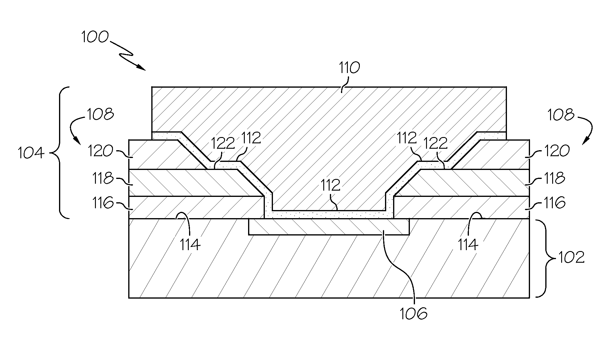
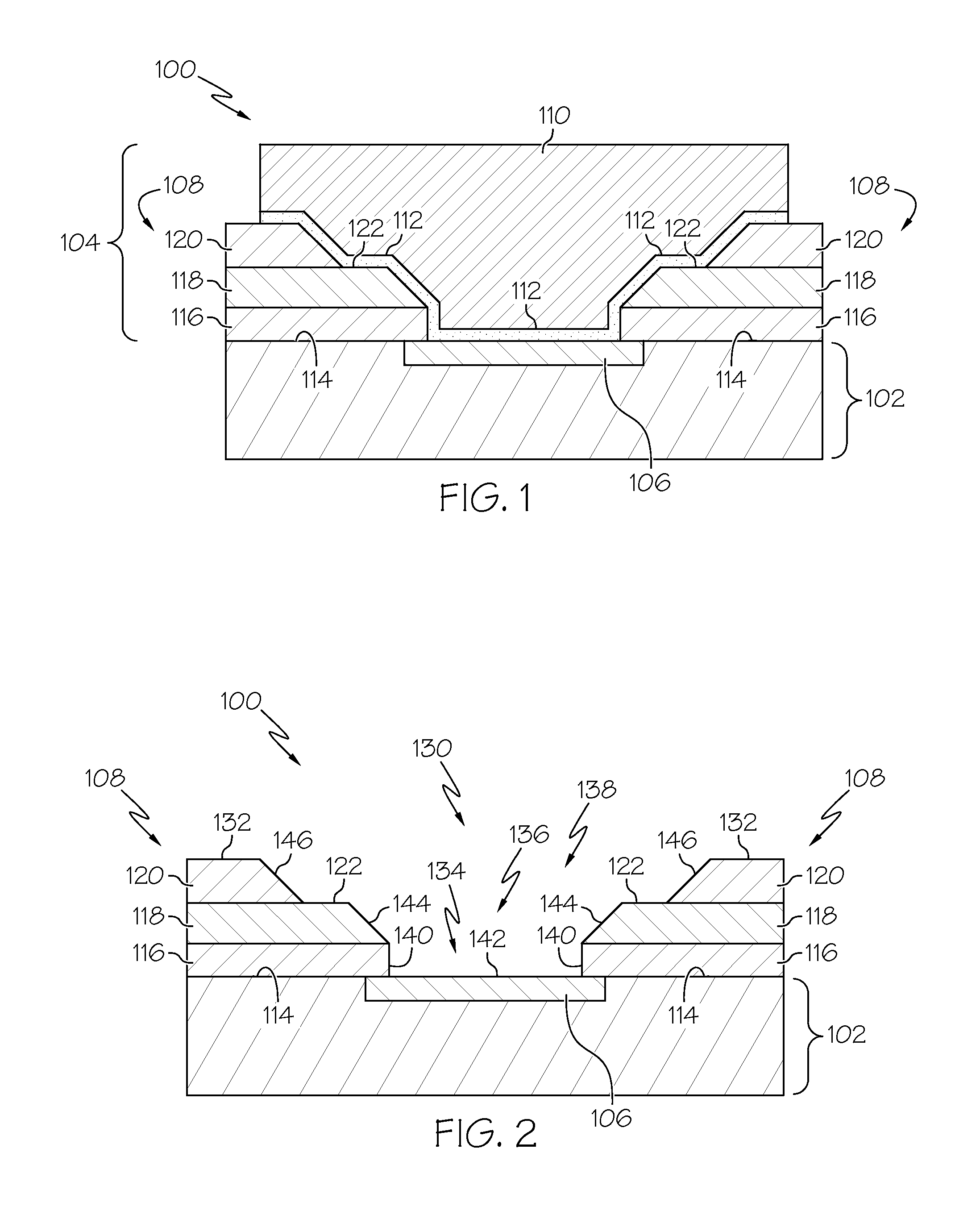
[0018]FIG. 1 is a cross-sectional view of an exemplary embodiment of a semiconductor device 100 that includes a semiconductor device structure 102 and a conductive connection structure 104 for the semiconductor device structure 102. Note that only a small portion of the semiconductor device 100 is shown in FIG. 1 (a realistic embodiment could include many conductive connection structures 104 arranged in an appropriate matrix or pattern). The semiconductor device structure 102 may be formed using conventional and well known semiconductor process technologies. In this regard, the semiconductor device structure 102 will typically include a support substrate, semiconductor material, dielectric material, and metal material in different layers (forming features such as transistors, conductive interconnects, isolation regions, conductive plugs, ILD, and the like). The semiconductor device structure 102 also includes a number of conductive contact pads that represent electrical connection p...

example

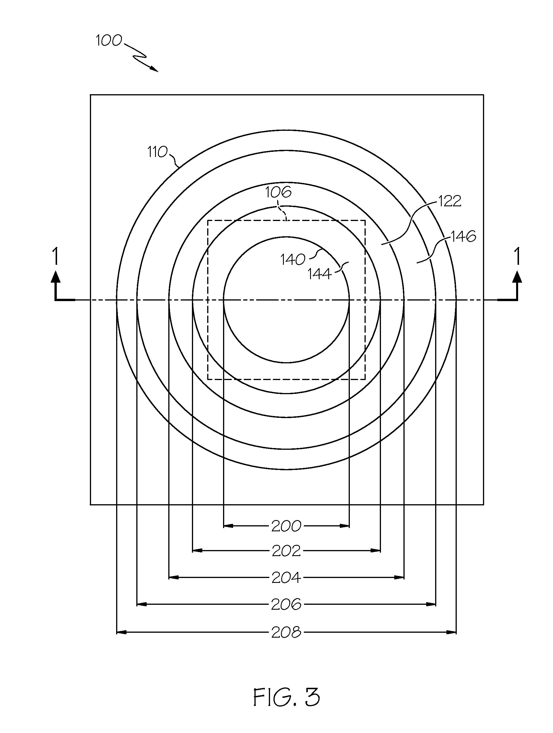
[0032]A preferred embodiment of the semiconductor device 100 may be fabricated with the following exemplary dimensions, which are not intended to be limiting of the disclosed subject matter in any way. This particular example corresponds to a solder bump that utilizes underbump metallization having a diameter of 105 μm. This diameter 208 is depicted in FIG. 3. For this 105 μm bump size, the lower stress buffer layer 118 and the upper stress buffer layer 120 are both 4 μm thick, and the passivation layer 116 is 900 nm thick. The sidewall slope defined in the lower stress buffer layer 118 is 40 degrees, and the sidewall slope defined in the upper stress buffer layer 120 is also 40 degrees.

[0033]For this example, the width of the square contact pad 106 is 5 μm, the diameter of the via 134 formed in the passivation layer 116 is 47 μm (reference number 200 in FIG. 3 corresponds to this dimension), the diameter at the top of the via 136 formed in the lower stress buffer layer 118 is 56 μm...

second embodiment

[0034]FIG. 4 is a cross-sectional view of another exemplary embodiment of a semiconductor device 400. A number of features and characteristics of the semiconductor device 400 are similar or identical to those described above for the semiconductor device 100 (for the sake of brevity, common features and characteristics will not be redundantly described here in the context of the semiconductor device 400). The semiconductor device 400 includes a semiconductor device structure 402 and a conductive connection structure 404 having a stress buffer arrangement 408 with a stepped profile. The conductive connection structure 404 includes a conductive connection element 410, underbump metallization 412, a passivation layer 416, a lower stress buffer layer 418, and an upper stress buffer layer 420.

[0035]The longitudinal cross-sectional profile of the stress buffer arrangement 408 includes a plurality of discrete steps (three vertical steps in this example). Notably, the stress buffer arrangeme...


PUM


Abstract

A semiconductor device disclosed herein includes a conductive connection structure having a stepped profile that serves as a stress relief feature. The conductive connection structure includes a stress buffer arrangement for a contact pad. The stress buffer arrangement has a stepped via that terminates at the contact pad, and the stepped via has a plurality of inwardly sloped and concentric sections in a stacked orientation. The connection structure also includes underbump metallization overlying at least a portion of the contact pad and lining the stepped via, and a conductive connection element coupled to the underbump metallization. The conductive connection element fills the lined recess.

Description

TECHNICAL FIELD[0001]Embodiments of the subject matter described herein relate generally to semiconductor devices and associated manufacturing processes. More particularly, embodiments of the subject matter relate to a conductive connection structure (suitable for solder bumps and conductive metal pillars) having improved stress reduction characteristics.BACKGROUND[0002]Semiconductor devices, integrated circuits, and related manufacturing and packaging techniques and processes are well known. A typical integrated circuit device includes a semiconductor device structure (e.g., a chip) that is packaged with appropriate leads and terminals for connecting the chip circuitry with the next assembly level, such as a circuit board, a carrier substrate, or the like. Some packaging approaches use conductive connection elements, such as solder bumps or copper pillars, that are electrically coupled to respective contact pads of the semiconductor device structure. The conductive connection eleme...

Claims


Application Information

Patent Timeline
Patent Type & Authority Applications(United States)
IPC IPC(8): H01L23/488H05K1/11H05K1/00H01L21/60
CPCH01L24/11H01L2924/01013H01L2924/01029H01L2924/01047H01L2924/01082H01L23/3192H01L24/03H01L24/05H01L24/13H01L2224/0345H01L2224/05541H01L2224/05555H01L2224/05558H01L2224/05639H01L2224/05647H01L2224/05655H01L2224/05666H01L2224/05684H01L2224/11462H01L2224/1147H01L2224/11849H01L2224/13022H01L2224/13111H01L2224/13147H01L2224/03912H01L2224/05572H01L2924/01019H01L2924/01033H01L2924/01074H01L2924/014H01L2924/00013H01L2224/0401H01L2924/00014H01L2924/2076H01L2224/13099H01L2224/13599H01L2224/05599H01L2224/05099H01L2224/29099H01L2224/29599H01L2924/14H01L2224/05018H01L2924/00
Inventor SCHULZE, THOMASKUECHENMEISTER, FRANKSU, MICHAELFU, LEI
Owner GLOBALFOUNDRIES INC
Why Eureka
Try Eureka