Adaptive lithographic critical dimension enhancement

a critical dimension and enhancement technology, applied in the field of lithographic system and method of lithographic exposure, can solve the problems of loss of yield, cd uniformity, affecting critical dimension uniformity, etc., and achieve the effect of improving cd uniformity

Inactive Publication Date: 2005-04-07
ASML NETHERLANDS BV
View PDF8 Cites 49 Cited by
  • Summary
  • Abstract
  • Description
  • Claims
  • Application Information

AI Technical Summary

Problems solved by technology

There are, however, numerous activities during the lithographic fabrication process that affect the critical dimension uniformity (CDU) and compromise the quality of the exposed pattern.
Such variations may occur across a target field, across a wafer, and between wafers and ultimately result in loss of yield.

Method used


Image

  • Adaptive lithographic critical dimension enhancement
  • Adaptive lithographic critical dimension enhancement
  • Adaptive lithographic critical dimension enhancement

Examples


Embodiment Construction

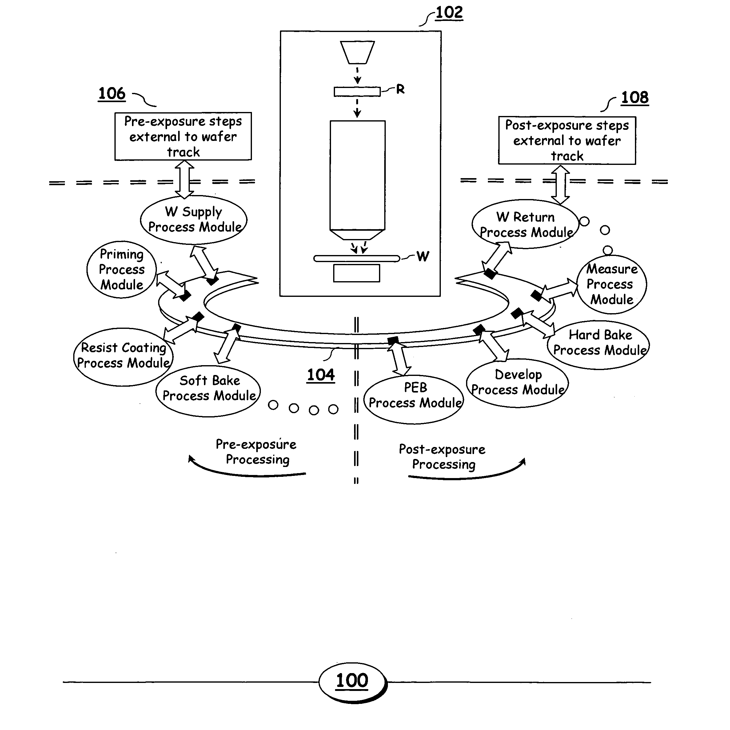
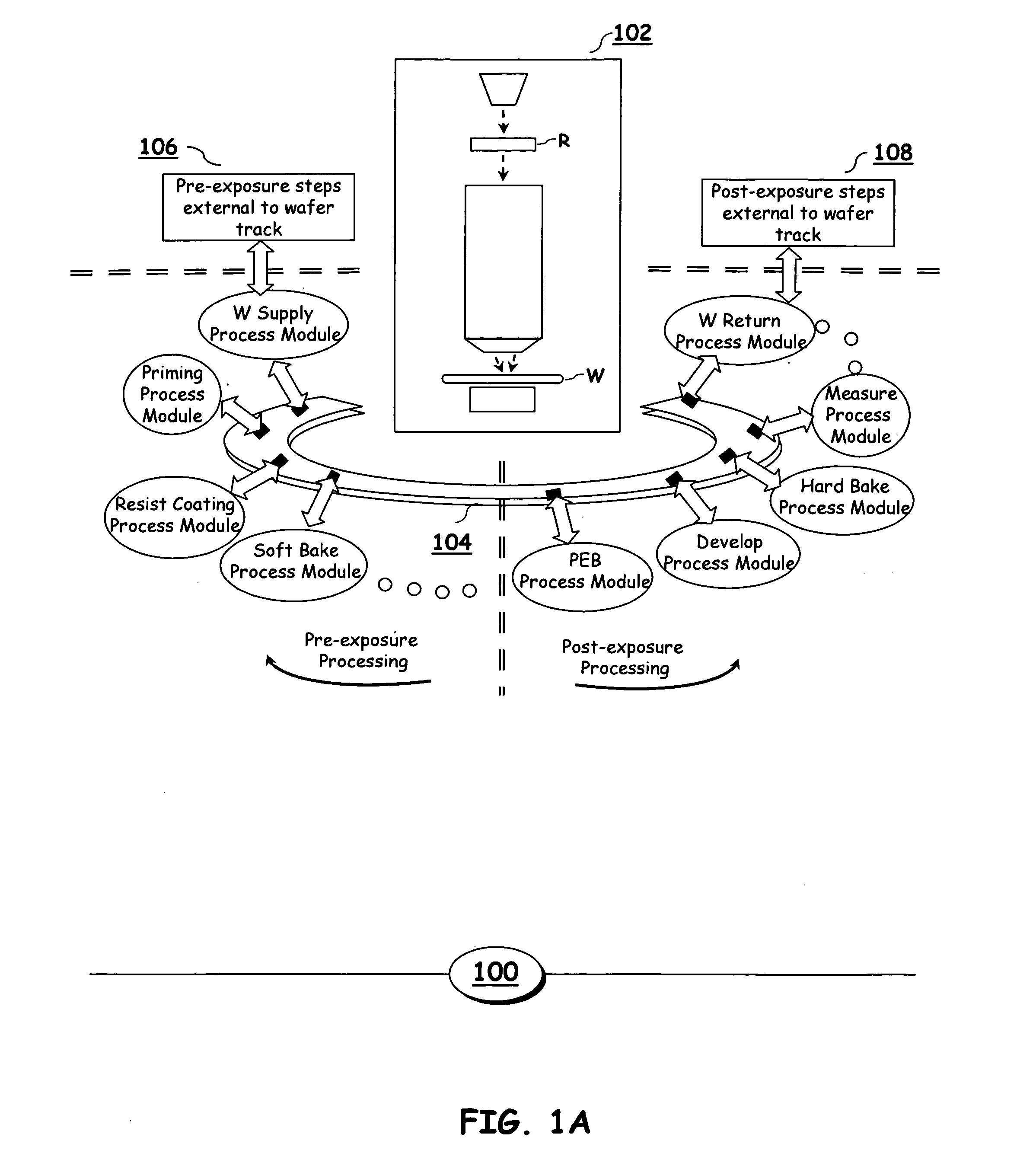
[0033] As noted above, processes that treat the substrate wafers contribute to variations in CDU that negatively affect the quality and performance of the exposed patterns. Such non-uniformities may occur across a target field, across a wafer, and between wafers. Moreover, these non-uniformities can also vary depending a variety of factors, such as the particular path the substrate wafer travels, scheduling anomalies, etc. As described in greater detail below, the present invention contemplates a lithographic system that employs an adaptive CD enhancement process whereby these variations and non-uniformities are factored out to provide acceptable CDU levels. Such a process exploits information regarding the lithographic system, for example, wafer track processing data, metrology data, and / or substrate wafer history data, to iteratively arrive at and maintain the optimal corrective dose offsets that improve overall CDU performance.

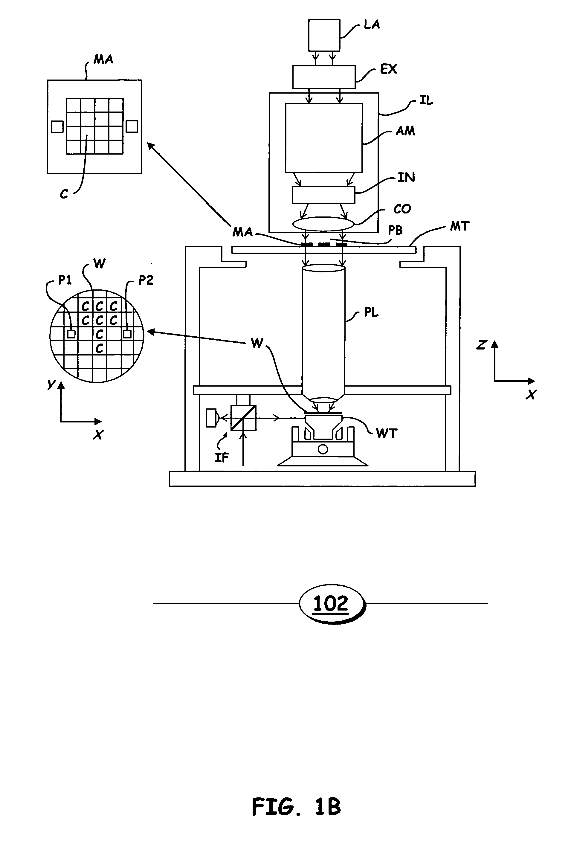
[0034]FIG. 1A schematically depicts lithographic sys...


PUM

PropertyMeasurementUnit
transmissionaaaaaaaaaa
reflectionaaaaaaaaaa
timeaaaaaaaaaa

Abstract

A system, apparatus, and method for improving CD uniformity in lithographic system is presented herein. The system includes an exposure apparatus configured to expose substrates, a track apparatus that is operatively coupled to the exposure apparatus and a plurality of processing modules and apparatus. The system also includes a measuring device configured to measure attributes of the exposed and processed substrates and to assess whether the exposed and processed substrate attributes are uniform based on pre-specified substrate profile information. The system further includes a module configured to adaptively calculate corrective exposure data based on the measured attributes upon determining that said attributes are not uniform. The corrective exposure data is configured to correct for non-uniformities in the substrates by regulating the exposure dosage of the exposure apparatus. Once the substrates are assessed to achieve the desired uniformity, the substrates are exposed by the exposure apparatus in accordance with the corrective exposure data, the uniformity of the exposed substrate continues to be monitored and the dose corrections are updated as required to maintain uniformity.

Description

BACKGROUND OF THE INVENTION [0001] 1. Field of the Invention [0002] The present invention generally relates to lithographic systems and methods of lithographic exposure. [0003] 2. Description of the Related Art [0004] The term “patterning means” as will be employed herein should be broadly interpreted to refer to means that can be used to endow an incoming radiation beam with a patterned cross-section, corresponding to a pattern that is to be created in a target portion of the substrate. The term “light valve” may also be used in this context. Generally, the pattern will correspond to a particular functional layer in a device being created in the target portion, such as an integrated circuit or other device (see below). Examples of such patterning means include: [0005] (a) a mask: the concept of a mask is well known in lithography, and it includes mask types such as binary, alternating phase-shift, and attenuated phase-shift, as well as various hybrid mask types. Placement of such a...

Claims


Application Information

Patent Timeline
Patent Type & Authority Applications(United States)
IPC IPC(8): H01L21/027G03F7/20
CPCG03F7/70558G03F7/70991G03F7/70625G03F7/705
Inventor PAXTON, THEODORE A.HIAR, TODD D.TEL, WIM T.DAVIS, TODD
Owner ASML NETHERLANDS BV
Why Eureka
Try Eureka