

Recessed gate transistor structure and method of forming the same
a transistor and recess technology, applied in the field ofmos transistors, can solve the problems of short or leakage current, gradual reduction of design rules for semiconductor devices, etc., and achieve the effect of reducing the height of the gate conductive layer and reducing the capacitan
- Summary
- Abstract
- Description
- Claims
- Application Information
AI Technical Summary
Benefits of technology
Problems solved by technology
Method used
Image

Examples
Embodiment Construction
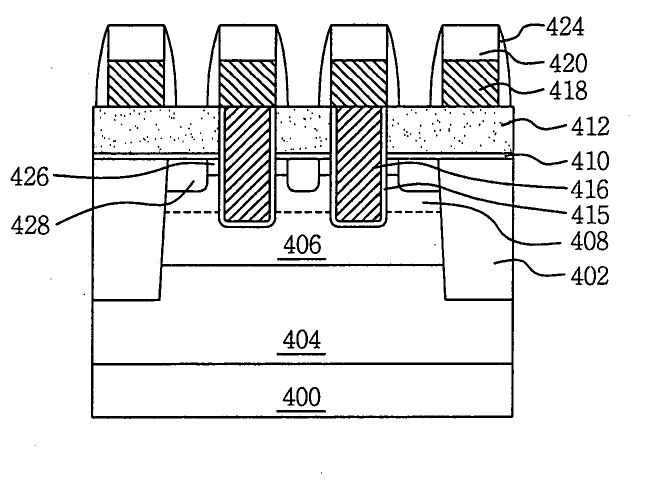
[0025] Preferred embodiments of the invention are described below in detail with reference to FIGS. 7 to 13. The invention may be embodied in many different forms and should not be construed as being limited to the embodiments set forth herein. Rather, these embodiments are provided so that this disclosure is thorough and complete, and to convey the concept of the invention to those skilled in the art.
[0026]FIG. 7 is a layout of a recessed gate transistor according to an embodiment of the invention. FIGS. 8 to 13 are cross-sectional views illustrating processes of forming a recessed gate transistor according to an embodiment of the invention.
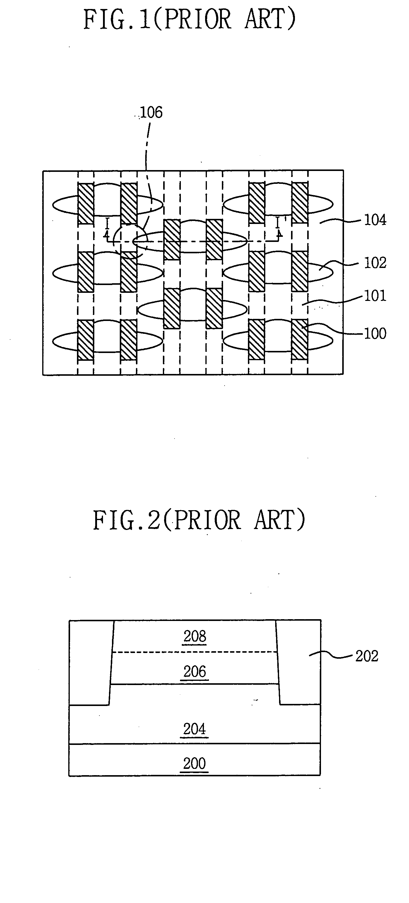
[0027] Referring first to FIG. 7, in order to fabricate several transistors simultaneously, two first-gate electrodes 301 patterned substantially parallel with each other are disposed substantially perpendicular to a length direction of each active region 302.
[0028] The adjacent active regions 302 are periodically arrayed in a staggered align...
PUM
 Abstract
Description
Claims
Application Information