Constant voltage power supply circuit
- Summary
- Abstract
- Description
- Claims
- Application Information
AI Technical Summary
Benefits of technology
Problems solved by technology
Method used
Image

Examples
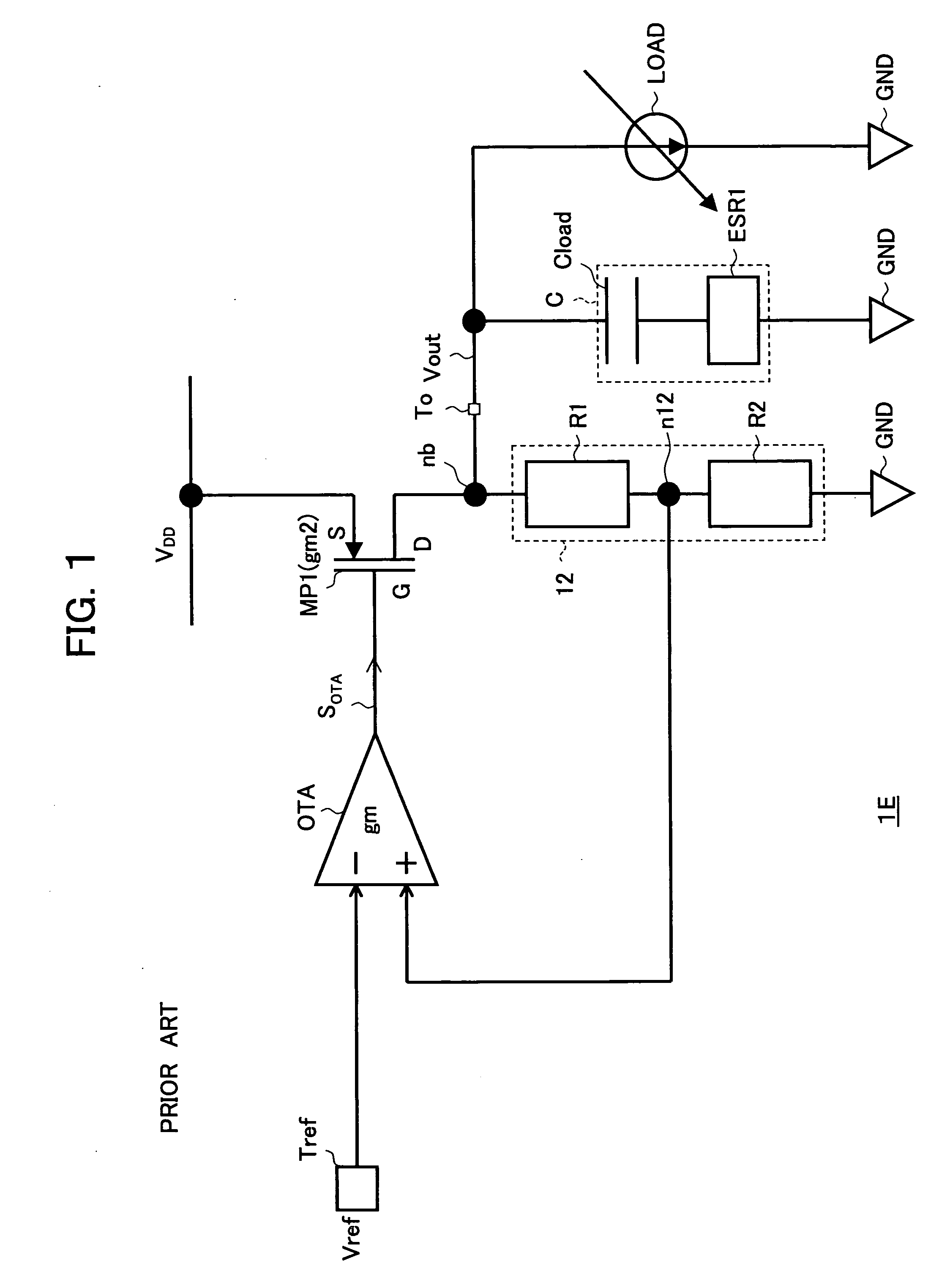
first embodiment
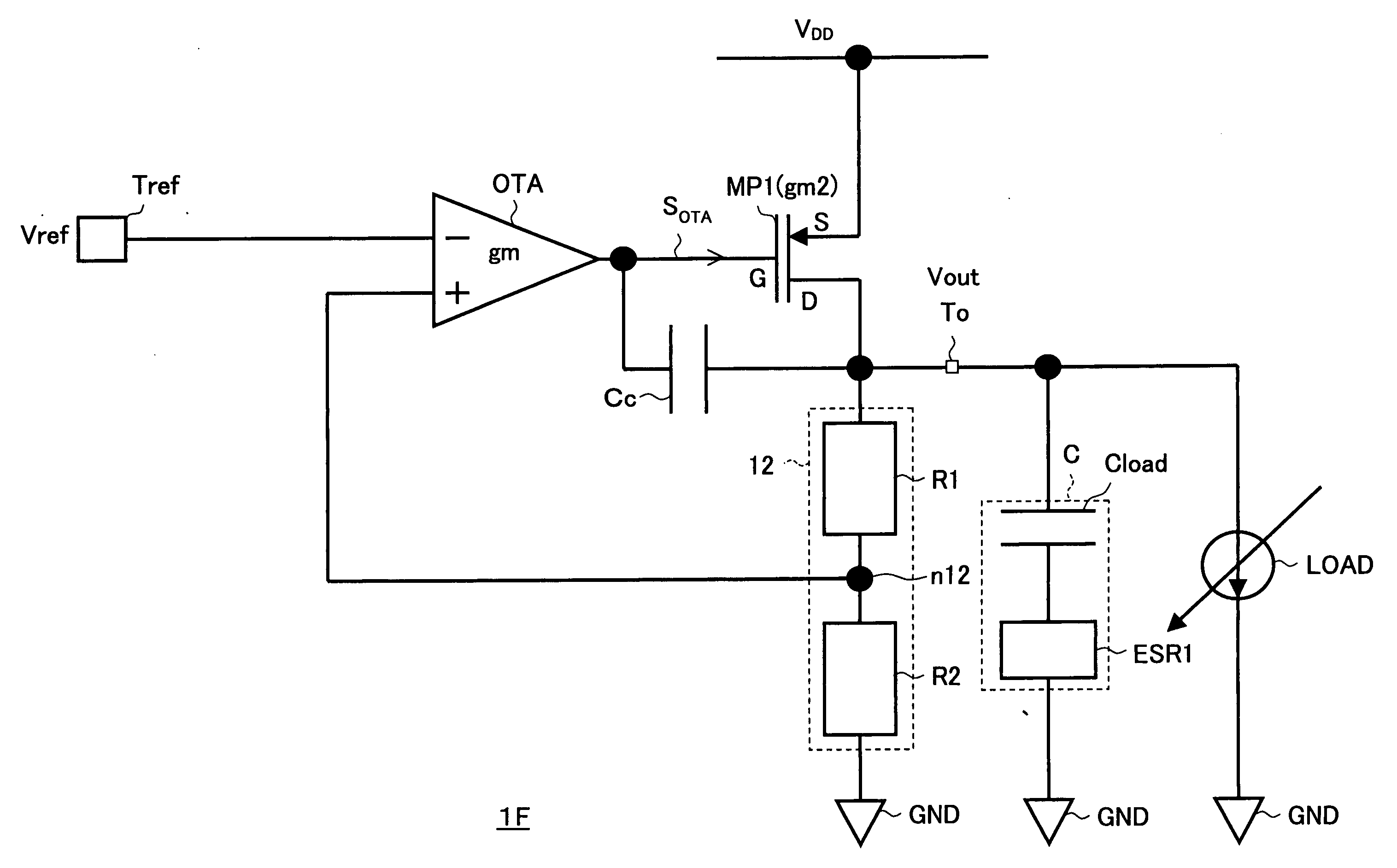
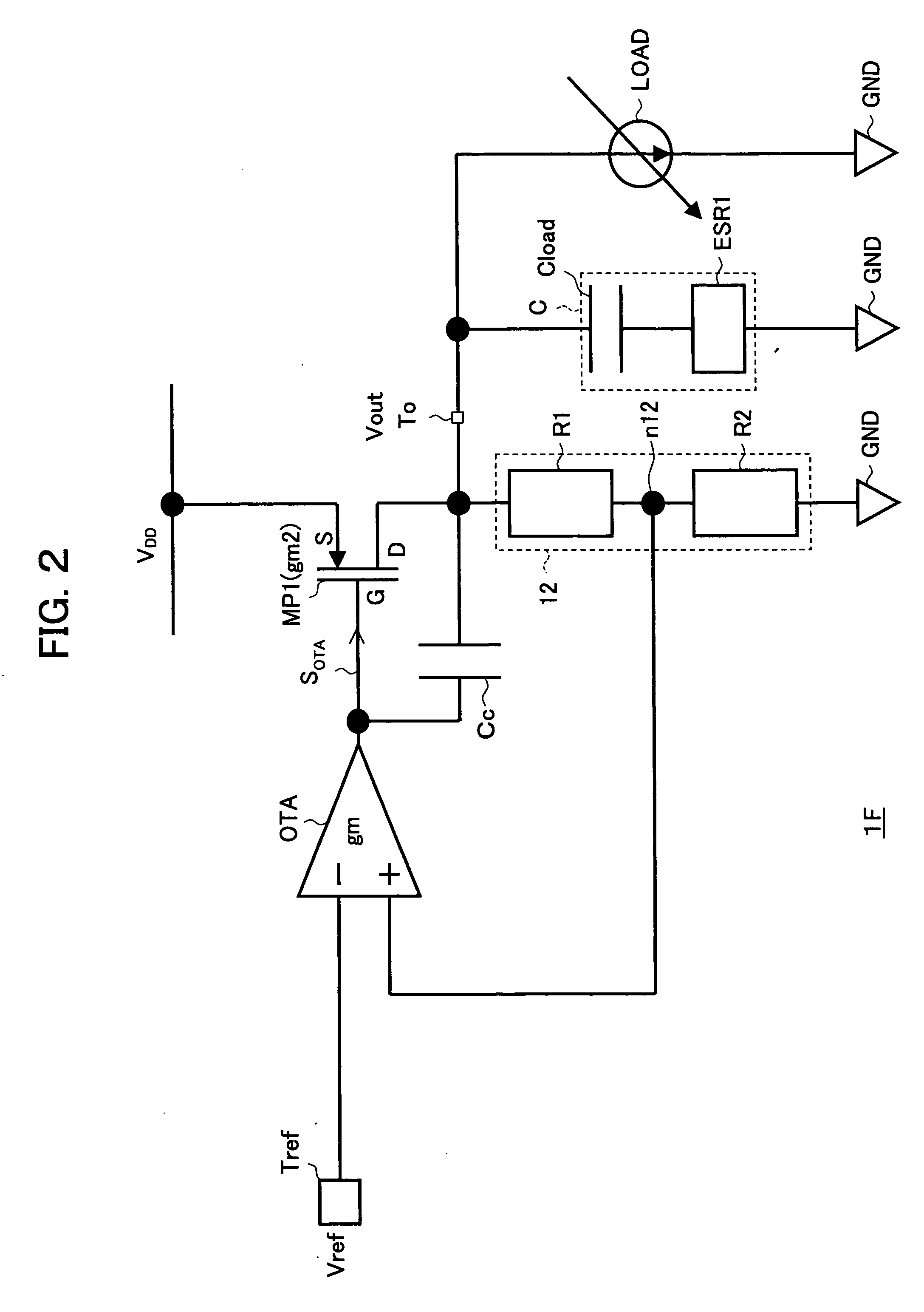
[0039] First Embodiment
[0040] A first embodiment will be described with reference to FIG. 2 to FIGS. 4A and 4B.
[0041]FIG. 2 is a circuit diagram showing a constant voltage supply circuit of a first embodiment of the present invention.
[0042] The difference between the constant voltage supply curcuit 1e in FIG. 1 and the constant voltage supply circuit 1f in FIG. 2 is the provision of a capacitor Cc for compensating a phase in the constant voltage supply circuit 1f in FIG. 2. Specifically, one terminal of the phase-compansating capacitor Cc is connected to the output terminal of the OTA and the gate G of the transistor MP1, and another terminal thereof is connected to the drain D of the transistor MP1.
[0043] It is supposed that, for the phase compansation, per se, the constant voltage supply circuit has a sufficient phase margin by a pole separation using a mirror compensation of the output transistor MP1, but it suffers from the disadvantages described later.
[0044]FIG. 3A is a gr...
second embodiment
[0053] Second Embodiment
[0054] A second embodiment of a constant voltage supply circuit of the present invention will be described with reference to FIG. 5.
[0055] The difference between the constant voltage supply circuit 1e and shown in FIG. 1 and the constant voltage supply circuit 1g shown in FIG. 5 is the provision of a phase compensation means performing the mirror compensation to the OTA (operational trans-conductance amplifier) in the constant voltage supply circuit 1g shown in FIG. 5. Only the differences will be described and the description of components having the same functions will be omitted.
[0056] The constant voltage supply circuit 1g shown in FIG. 5 has an OTA (operational trans-conductance amplifier) including an amplifier AMP, a P-type MOSFET transistor MP2, an N-type MOSFET transistor MN3, and a phase-compensating capacitor CC.
[0057] The amplifier AMP is a differential-operation type amplifier circuit, an inverted input terminal thereof is connected to the ref...
third embodiment
[0063] Third Embodiment
[0064] A third embodiment of a constant voltage power circuit according to the present invention will be described with reference to FIG. 6 to FIGS. 9A and 9B.
[0065] The constant voltage power supply circuit 1 shown in FIG. 6 is called as a low drop-out regulator (regulation circuit) and includes an output controlling transistor MP1 of a P-type MOSFET, an operational amplifier circuit 11, a voltage-dividing circuit 12, a phase-compensating capacitor CC, and an output capacitor C.
[0066] The operational amplifier circuit 11 includes an operational trans-conductance amplifier (OTA), current mirror circuits CM1 to CM3, an N-type MOSFET transistor MN4, and an N-type MOSFET transistor MN5. The transistors MN4 and MN5 are optional, however, to improve an offset, a gain, etc., the provision of these transistors are preferable.
[0067] The voltage-dividing circuit 12 includes series connected resistor elements R1 and R2.
[0068] The output capacitor C includes a capaci...
PUM
 Abstract
Description
Claims
Application Information
 - Generate Ideas
- Intellectual Property
- Life Sciences
- Materials
- Tech Scout
- Unparalleled Data Quality
- Higher Quality Content
- 60% Fewer Hallucinations
Browse by: Latest US Patents, China's latest patents, Technical Efficacy Thesaurus, Application Domain, Technology Topic, Popular Technical Reports.
© 2025 PatSnap. All rights reserved.Legal|Privacy policy|Modern Slavery Act Transparency Statement|Sitemap|About US| Contact US: help@patsnap.com