Apparatus and method for discovering a scratch pad memory configuration

Active Publication Date: 2005-05-12
ARM FINANCE OVERSEAS LTD
View PDF14 Cites 42 Cited by
  • Summary
  • Abstract
  • Description
  • Claims
  • Application Information

AI Technical Summary

Benefits of technology

[0008] The invention also includes a processor probe. The processor probe has input/output circuitry and control logic connected to the input/output circuitry. A scratch pad configuration query module is connected to the control logic. The scratch pad configuration query module is configured to initiate, in conjunction with the co

Problems solved by technology

These unique configurations lead to problems in debugging embedded processor systems.
A limitation associated with these tools is that they require information on the config

Method used


Image

  • Apparatus and method for discovering a scratch pad memory configuration
  • Apparatus and method for discovering a scratch pad memory configuration
  • Apparatus and method for discovering a scratch pad memory configuration

Examples


Embodiment Construction

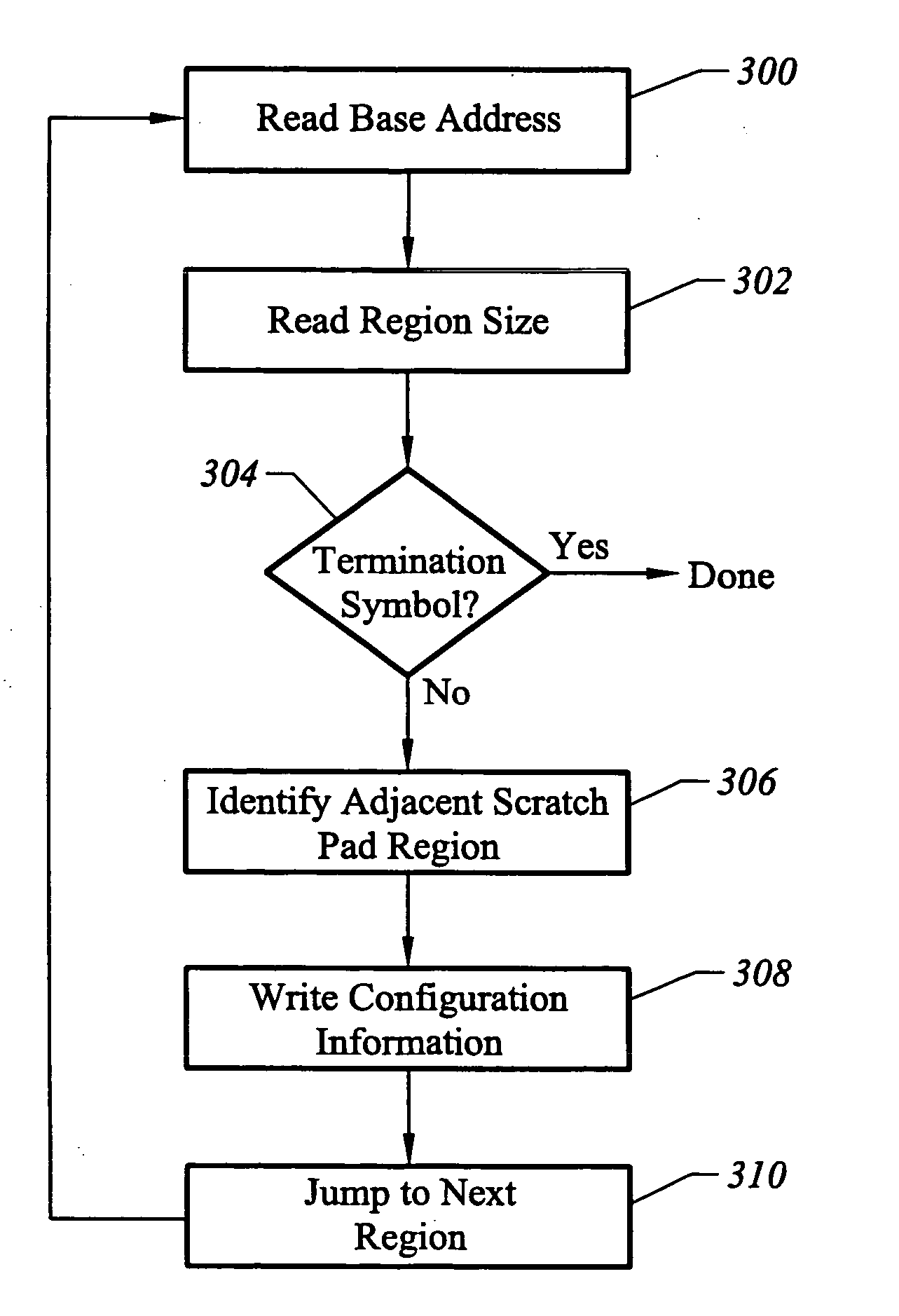
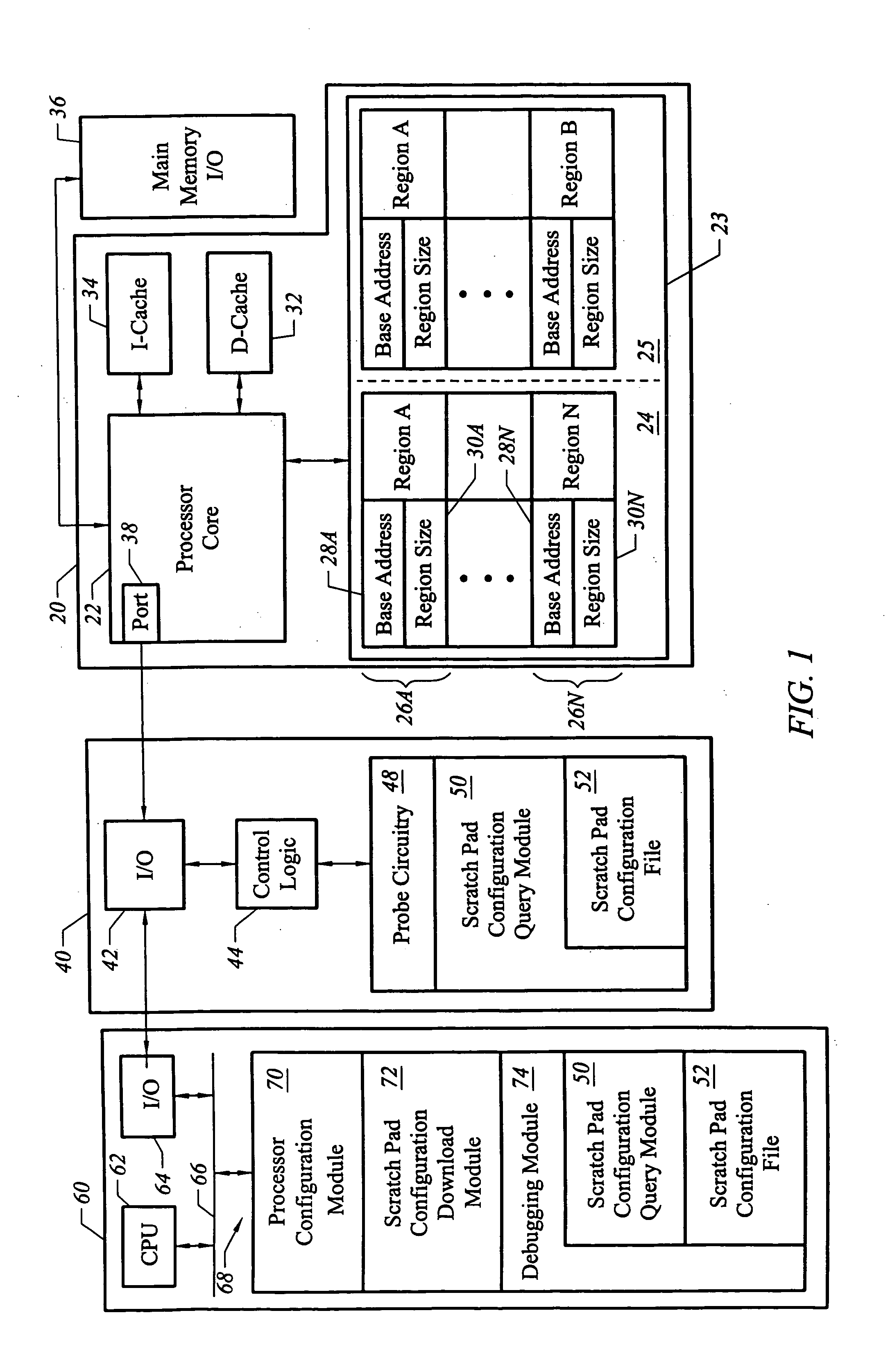
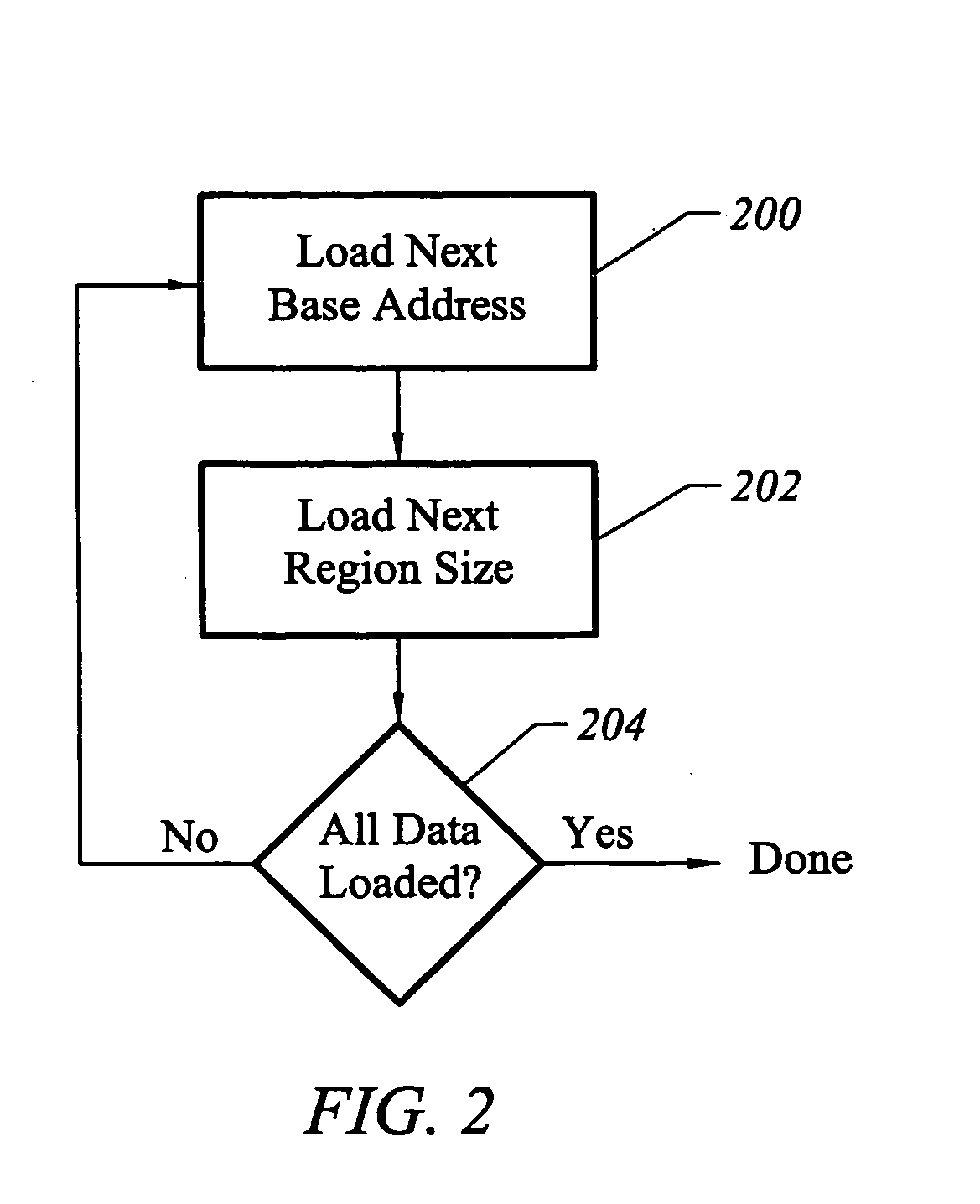
[0019]FIG. 1 illustrates an embedded processor 20 configured in accordance with an embodiment of the invention. The embedded processor 20 includes a processor core 22. The embedded processor 22 is in communication with a scratch pad memory 23. In one embodiment, the scratch pad memory 23 includes an instruction scratch pad 24 and a data scratch pad 25. The instruction scratch pad 24 and the data scratch pad 25 of the scratch pad memory 23 each include a set of scratch pad regions 26A-26N.

[0020] The scratch pad regions are configurable by a customer that purchases a processor core 22. That is, when purchasing or licensing a processor core design for an embedded system, various scratch pad configurations can be defined, depending upon the application. In accordance with the invention, configuration of the scratch pad is made visible to debugging software or another application by loading a base address 28 and region size 30 for each scratch pad region 26. Thus, FIG. 1 illustrates bas...


PUM


Abstract

The invention includes a method of debugging an embedded processor. Scratch pad memory of an embedded processor is accessed to form a configuration file characterizing the configuration of scratch pad regions of the scratch pad memory. The embedded processor is debugged using information from the configuration file. The invention also includes an embedded processor with a processor core and scratch pad memory connected to the processor core. The scratch pad memory includes a set of scratch pad regions. The scratch pad memory stores values characterizing base addresses and region size values of the set of scratch pad regions.

Description

BRIEF DESCRIPTION OF THE INVENTION [0001] This invention relates generally to embedded processors. More particularly, this invention relates to a technique for identifying a scratch pad memory configuration associated with an embedded processor. BACKGROUND OF THE INVENTION [0002] An embedded processor is an electronic control and computation device incorporated into an engineered system, such as a camera, game console, printer, personal digital assistant, and the like. An embedded processor has a processor core and an associated memory. The associated memory commonly includes a scratch pad memory, which is a general-purpose random access memory region for the processor core. The patent application entitled “Scratch Pad RAM with Cache-Like Access Times”, Ser. No. 09 / 494,488, filed Jan. 31, 2000, and assigned to the assignee of the present invention, describes a technique for accessing scratch pad memory. The contents of the application are incorporated herein. The memory associated w...

Claims


Application Information

Patent Timeline
IPC IPC(8): G06F12/06
CPCG06F12/0684
Inventor KINTER, RYAN C.MCCOY, SCOTT M.INTRATER, GIDEON D.
Owner ARM FINANCE OVERSEAS LTD
Why Eureka
Try Eureka