

Partial bank DRAM refresh
a dram and partial bank technology, applied in the field of dynamic random access memory (dram), can solve the problems of unread data, unacceptable refresh overhead, increase the latency of any read,
- Summary
- Abstract
- Description
- Claims
- Application Information
AI Technical Summary
Benefits of technology
Problems solved by technology
Method used
Image

Examples
Embodiment Construction
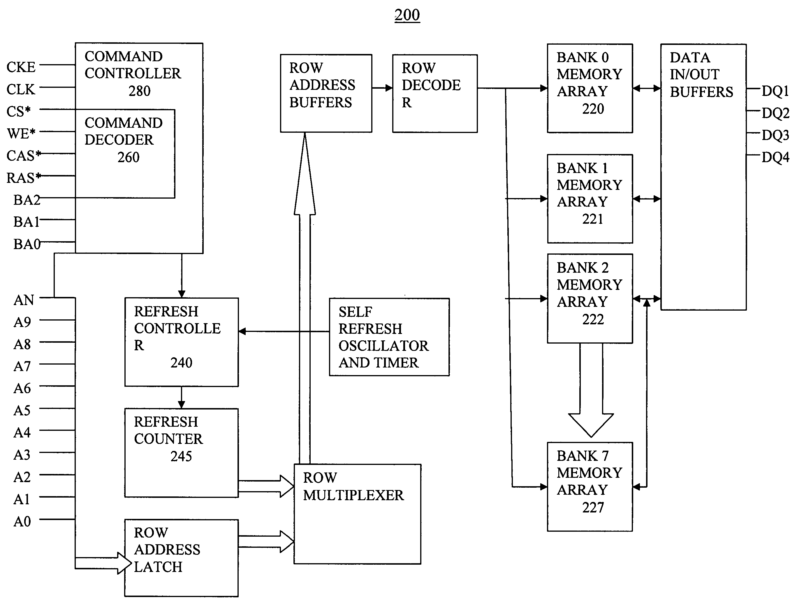
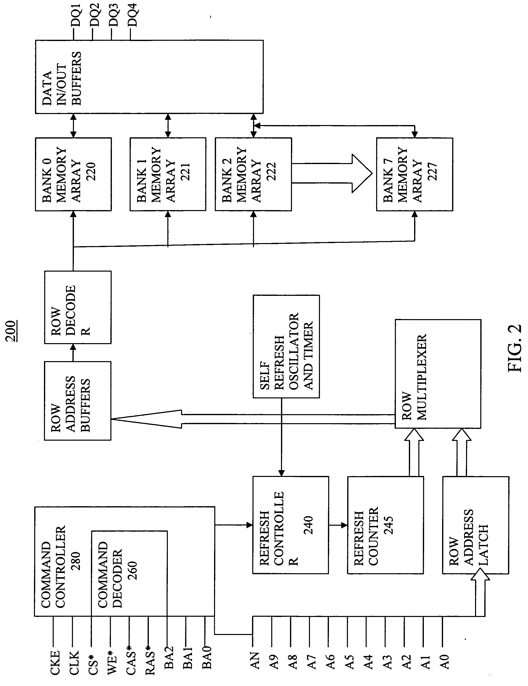
[0018] The present invention improves the performance of memory subsystems by providing a method to refresh a fraction of the banks in a DRAM in response to a given refresh command. Refreshing a fraction of the banks allows a degree of concurrency with reads and / or writes to the remaining banks in the DRAM which are not being refreshed. Additional performance may be gained because it is not necessary to close the pages of the banks that are not being refreshed, potentially reducing the read latency to the data in those banks. In embodiments of the present invention each refresh command refreshes half of the banks in the DRAM. For example, in one embodiment, each refresh command (refreshing half of the banks in the DRAM) does half as much work as an all-bank refresh command (for the same number of rows per bank), so that twice as many refresh commands are needed per refresh period tREF. In a second embodiment, the number of refresh commands per refresh period tREF stays the same as a...
PUM
 Abstract
Description
Claims
Application Information