Electro-optical device, manufacturing method of the same, and electronic apparatus

a manufacturing method and electronic technology, applied in the direction of transistors, electroluminescent light sources, electric lighting sources, etc., can solve the problems of external stress concentrates, thin film cracks or peeling off, deterioration of shielding properties, etc., to prevent peeling or cracking, the effect of deterioration of light emitting layers

Active Publication Date: 2005-05-26
SEIKO EPSON CORP
View PDF2 Cites 85 Cited by
  • Summary
  • Abstract
  • Description
  • Claims
  • Application Information

AI Technical Summary

Benefits of technology

This patent describes how to create an electronic device with good protection against cracks and damage caused by external factors such as water. By adding a buffer layer that has more height than the actual components, this prevents stresses from accumulating and causing failure. Additionally, a gas barrier layer is added over the buffer layer to further protect against moisture and other contaminants. These measures result in better durability and longer lifespan for the electronic devices made through this process.

Problems solved by technology

The technical problem addressed in this patent text relates to improving the durability of electronic optical devices, particularly those containing sensitive components such as organic luminescent displays, against damage caused by environmental factors including oxygen and water. This can result in reduced performance lifetimes for these devices. Various techniques have been developed over time to address this issue, including the use of protective lids and coatings, but more recent advancements focus on employing thinner and higher quality films to better prevent moisture penetration and corrosion.

Method used


Image

  • Electro-optical device, manufacturing method of the same, and electronic apparatus
  • Electro-optical device, manufacturing method of the same, and electronic apparatus
  • Electro-optical device, manufacturing method of the same, and electronic apparatus

Examples


first embodiment

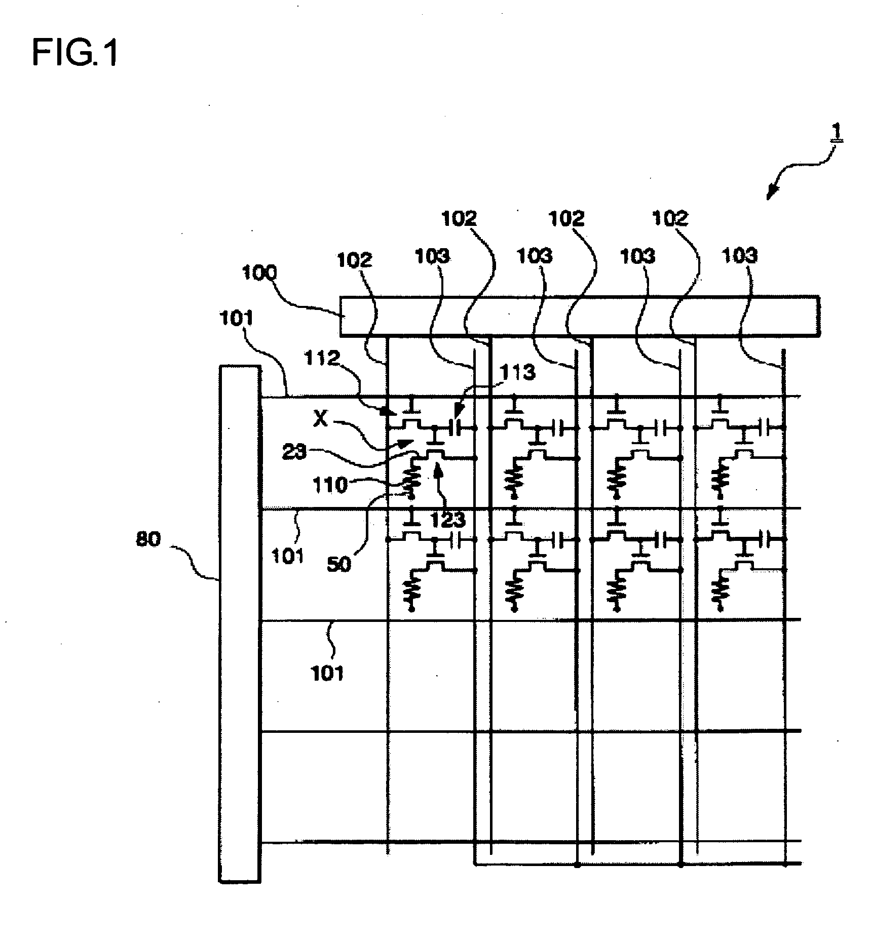
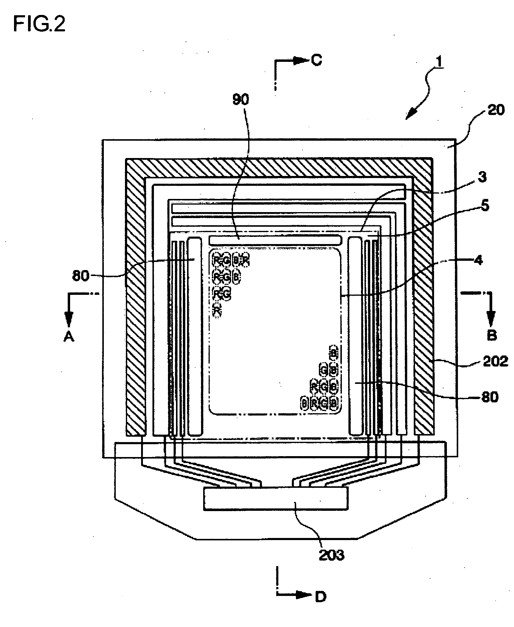
[0087]FIG. 1 shows the wiring configuration of an EL display device 1. The EL display device I is an active matrix type EL display device containing thin film transistors (hereinafter, abbreviated to TFT) as switching elements.

[0088] Referring to the wiring-configuration of the EL display device (electro-optical device) 1, a plurality of scanning lines 101, a plurality of signal lines 102 extended in such a direction as to intersect the respective scanning lines 101 at a right angle, and a plurality of power-supply lines 103 which are extended in parallel to the signal lines 102 are arranged. Moreover, pixel regions X are provided near the intersecting points of the scanning lines 101 and the signal lines 102, respectively.

[0089] A data line drive circuit 100 provided with a shift register, a level shifter, a video line, and an analog switch is connected to the signal lines 102. A scanning line drive circuit 80 having a shift register and a level shifter is connected to the scanni...

second embodiment

[0213] Hereinafter, a second embodiment of the EL display device will be described. The same members, positions, and elements as those of the first embodiment are designated by the same reference numerals. The description thereof is not repeated.

[0214] The EL display device 6 uses a frame 216 instead of the frame 215 of the EL display device 1. The frame 216 is formed with the same material as that for the organic bank layers 221. Since the frame 216 and the organic bank layers 221 are formed with the same materials, both of them can be produced by the same process. Thus, the production process or the like can be simplified.

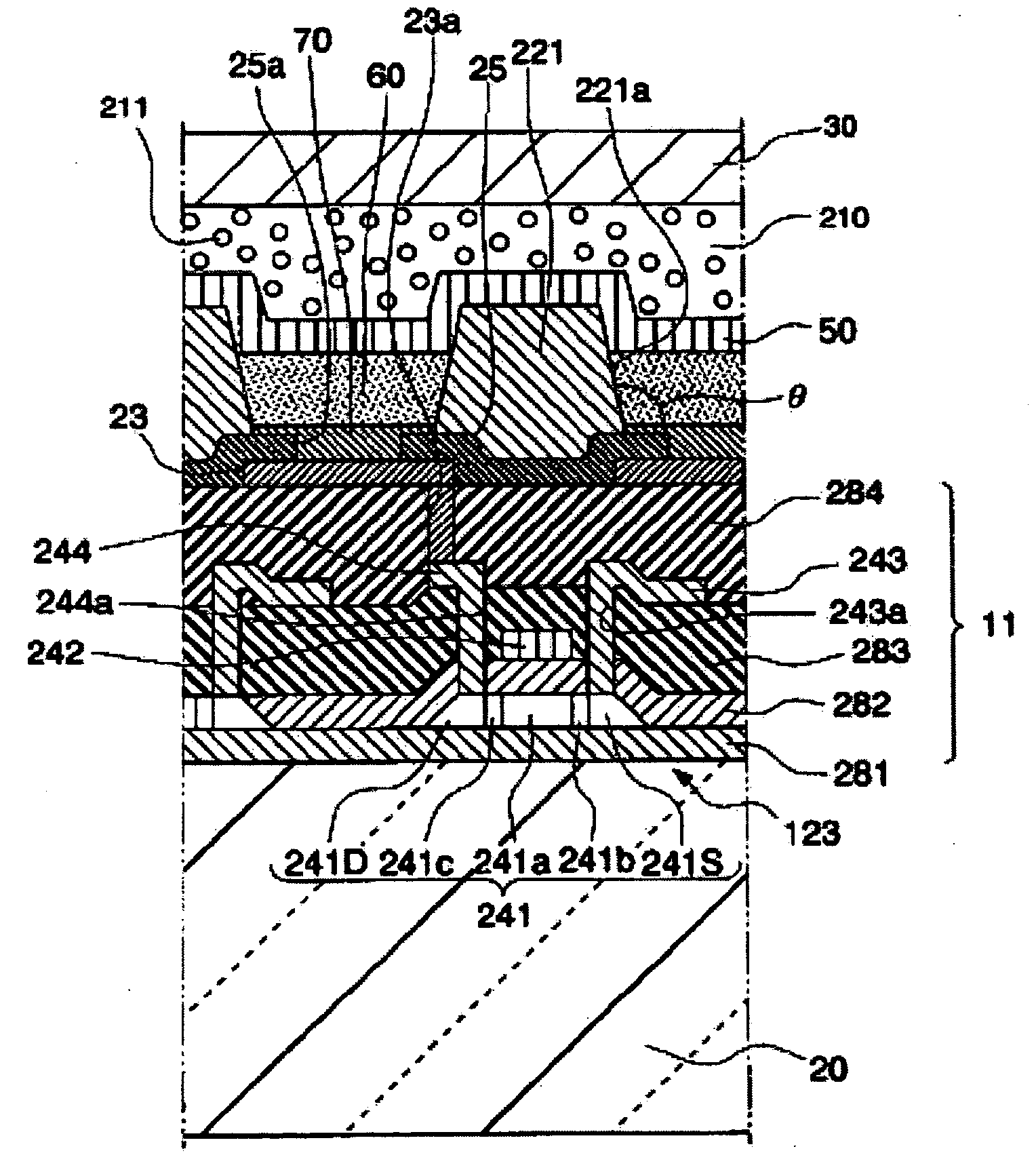
[0215] In the EL display device 6, a plurality of light emitting elements (organic EL elements) having the pixel electrodes 23, the organic light emitting layers 60, and the cathodes 50 are formed on the substrate 200, and moreover, the buffer layer 210 is formed so as to cover the light emitting elements. Moreover, the frame 216 is formed so as to surround the...

third embodiment

[0246] Hereinafter, a third of the EL display device will be described. The same members, positions, and elements as those of the first and second embodiments are designated by the same reference numerals. The description thereof is not repeated.

[0247] The EL display device 7 uses a liquid repellent layer 217 instead of the frames 215 and 216. The frames 215 and 216 are mechanical members which dam the buffer layer material, i.e., prevent the material from flowing out of the predetermined area. On the other hand, the liquid repellent layer 217 dams the buffer layer material from flowing out of the predetermined area by utilization of chemical action.

[0248] In the EL display device 7, a plurality of light emitting elements (organic EL elements) having the pixel electrodes 23, the organic light emitting layers 60, and the cathodes 50 are formed on the substrate 200, and moreover, the buffer layer 210, the gas barrier layer 30, and so forth are formed so as to cover the light emittin...


PUM


Abstract

To provide an electro-optical device having a buffer layer which planarizes a gas barrier layer so that stress-concentration in the gas barrier layer is reduced, the buffer layer being prevented from leaking out of a predetermined area, and to provide a method of producing the same and an electronic apparatus. In an electro-optical device 1 having, on a substrate 200, a plurality of first electrodes 23, a bank structure 221 having a plurality of openings 221a positioned correspondingly to the formed first electrodes, electro-optical layers 60 arranged in the respective openings 221a, and a second electrode 50 covering the bank structure 221 and the electro-optical layers 60, the device includes a buffer layer 210 formed so as to cover the second electrode 50 and have a substantially flat upper surface, a frame 215 made of a material having no affinity to the buffer layer 210 and surrounding the periphery of the buffer layer 210, and a gas barrier layer 30 covering the buffer layer 210 and the frame 215.

Description


Claims


Application Information

Patent Timeline
Owner SEIKO EPSON CORP
Why Eureka
Try Eureka