Method and apparatus for inspecting defects of patterns

a pattern and defect technology, applied in the field of pattern defect inspection and foreign material inspection, can solve the problems of high peak power of lasers, difficult to detect by conventional technology, non-visual defects, etc., and achieve the effects of reducing the amount of light unevenness, and reducing the damage caused by illumination ligh

Inactive Publication Date: 2005-05-26
HITACHI HIGH-TECH CORP
View PDF7 Cites 61 Cited by
  • Summary
  • Abstract
  • Description
  • Claims
  • Application Information

AI Technical Summary

Benefits of technology

[0011] According to this invention, damage on the wafer caused by the illumination light can be reduced, the coherence of the laser light can be reduced, and further output of the grain can be stabilized while reducing amount-of-light unevenness from a part of the insulator film in the wiring process etc. In addition, it becomes possible to perform parallel detection by dividing a range of visual field without causing a loss, and hence high-speed and high-sensitivity inspection of a wafer in each step becomes possible.

Problems solved by technology

Especially, there is also reported a defect, called “Non Visual Defect,” that is hard to detect by the conventional technology.
However, the pulsed lasers have high peak powers, so it is very likely that a sample irradiated by that laser light might be damaged.
However, in this case, it is necessary to lengthen storage time of an image sensor for detecting reflected light because of insufficient amount of light irradiated on the sample, and hence this measure comes with a problem of incompatibility with high-speed inspection.
When high-speed inspection is intended, an illumination method of scanning a narrowly converged laser beam on a sample is not suitable.
Conversely, if a laser beam that is expanded as large as the whole visual field is used for illumination, there occurs speckle by the laser and signals of overshoot and undershoot, called ringing, are generated in edge parts of a circuit pattern; therefore, it is difficult to obtain a high-quality image, and otherwise it is necessary to reduce interference by the laser light.
Moreover, in the LSI device, structures of patterns to be inspected have become complicated and diversified, such as memory products formed mainly with a repeated pattern and logic products formed mainly with a non-repeated pattern, so it is difficult to find targeted defects surely.
Furthermore, in the process of metal wiring, such as of Al (aluminum), minute irregularities called grain, pit, and morphology occur.
Because this grain is detected as an optical noise during inspection, there is a problem that detected grain must be reduced.
Moreover, in any process in which a transparent film (here, a term transparent is used to mean “being transparent at illumination wavelength”), such as an insulator film, is exposed as an uppermost layer, interference-light intensity unevenness arising from a minute difference in thickness of the transparent film causes optical noise.
Therefore, there is a problem that the optical noise must be reduced.

Method used


Image

  • Method and apparatus for inspecting defects of patterns
  • Method and apparatus for inspecting defects of patterns
  • Method and apparatus for inspecting defects of patterns

Examples


embodiment 2

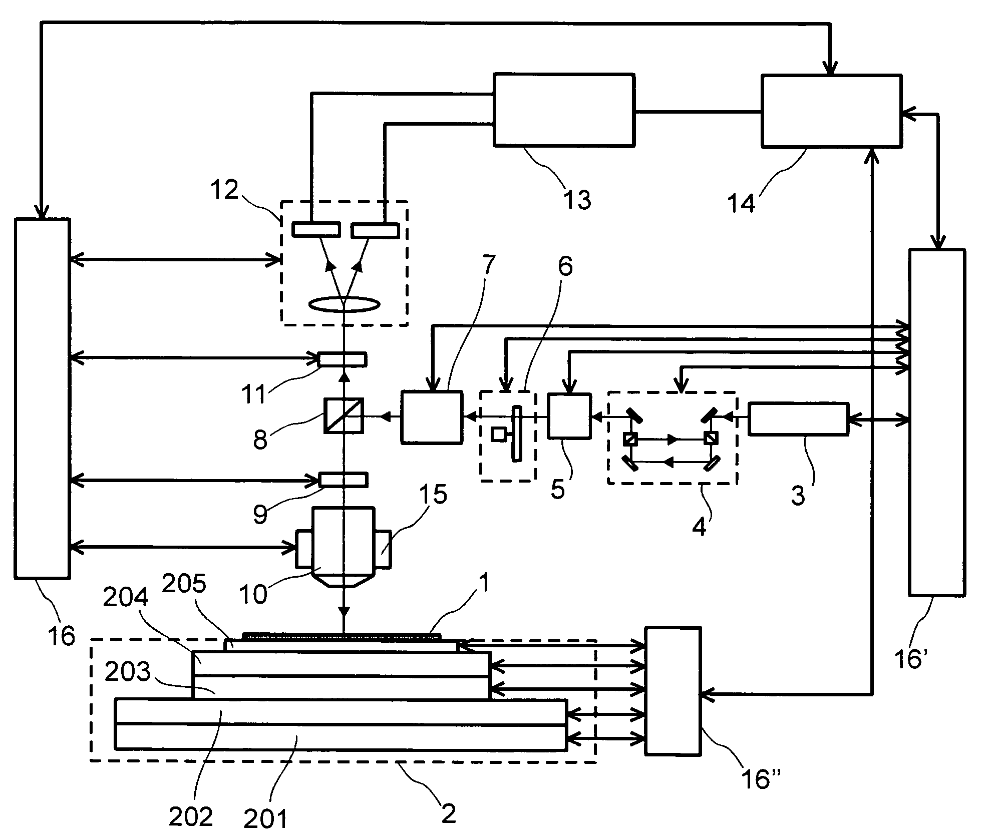
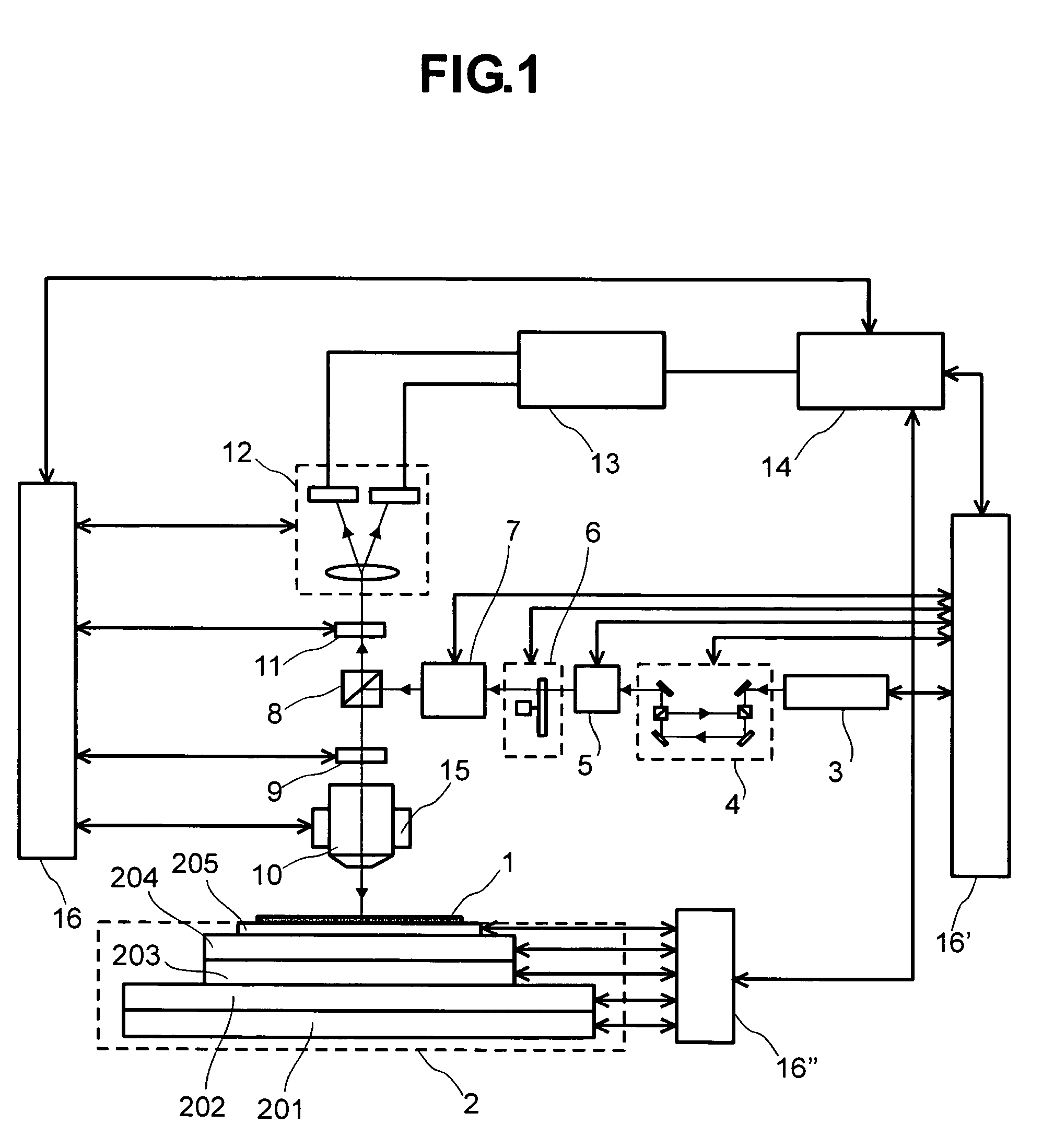
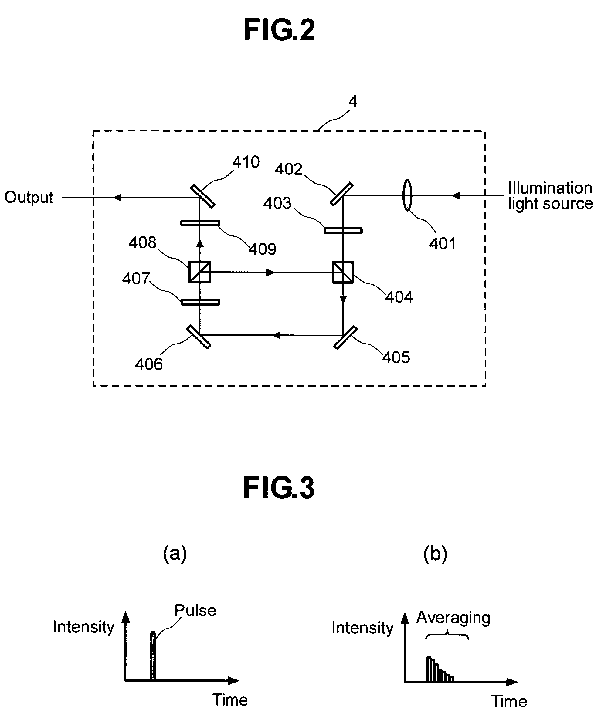
[0124] Another embodiment of a pattern-defect inspection apparatus according to this invention is shown in FIG. 26. The pattern-defect inspection apparatus of this embodiment consists of: the conveyance system 2 for placing and moving the wafer 1 to be inspected, the illumination light source 3, the pseudo continuous-wave forming optical system 4, the beam formation optical system 5, the coherence reduction optical system 6, the deformation illumination optical system 7, the PBS 8, the light modulation unit A 9, the objective lens 10, the light modulation unit B 11, the visual-field divided parallel detection unit 12, the signal processing circuit 13, the I / O unit 14, the A / F unit 15, a polarized-light dark-field illumination optical system A 18, a polarized-light dark-field illumination optical system B 19, and controllers, relay lenses, and mirrors of the units not shown in the figure.

[0125] Next, its operation will be described. The illumination light emitted from the illuminati...

embodiment 3

[0140] Another embodiment of the pattern-defect inspection apparatus according to this invention is shown in FIG. 34. The pattern-defect inspection apparatus of this embodiment consists of: the conveyance system 2 for placing and moving the wafer 1 to be inspected, the illumination light source 3, the pseudo continuous-wave forming optical system 4, the beam formation optical system 5, the coherence reduction optical system 6, the deformation illumination optical system 7, the PBS 8, the light modulation unit A 9, the objective lens 10, the light modulation unit B 11, the visual-field divided parallel detection unit 12, the signal processing circuit 13, the I / O unit 14, the A / F unit 15, an illumination light source 20 having a wavelength different from that of the illumination light source 3, a dichroic prism 21, and controllers, relay lenses, and mirrors of the units not shown in the figure.

[0141] Next, its operation will be described. The illumination light of a wavelength λ1 emi...

embodiment 4

[0146] Another embodiment of the pattern-defect inspection apparatus according to this invention is shown in FIG. 36. The pattern-defect inspection apparatus of this embodiment is constructed with: an oil-immersion conveyance system 22 for moving the wafer 1 to be inspected that is placed thereon while being immersed in a medium 2213, the illumination light source 3, the pseudo continuous-wave forming optical system 4, the beam formation optical system 5, the coherence reduction optical system 6, the deformation illumination optical system 7, the PBS 8, the light modulation unit A 9, an objective lens 10′, the light modulation unit B 11, the visual-field divided parallel detection unit 12, the signal processing circuit 13, the I / O unit 14, and the A / F unit 15, as well as controllers, relay lenses, and mirrors of the units not shown in the figure. The objective lens 10′ differs from the objective lens 10 shown in FIG. 1 in that it has a sealed structure such that the medium 2213 does...


PUM

PropertyMeasurementUnit
widthsaaaaaaaaaa
wavelengthaaaaaaaaaa

Abstract

Disclosed is a method and apparatus for inspecting defects of patterns of a sample at high speed and with high sensitivity while damage of the sample arising from high-power pulsed light is reduced. Light emitted from a pulsed laser light source is transmitted through a pseudo continuous-wave forming optical system having an optical system capable of reducing energy per pulse and yet maintaining the entire amount of light of the pulsed light, a beam formation optical system, and a coherence reduction optical system, and a beam deflected by a deformation illumination optical system is made to reflect on a PBS to be irradiated on a wafer. The apparatus is configured so that the diffracted light from the wafer is focused by an objective lens, transmitted through light modulation units, focused to form a plurality of images on a plurality of image sensors in a visual-field divided parallel detection unit 12, and then defects are detected by a signal processing unit.

Description

BACKGROUND OF THE INVENTION [0001] The present invention relates to pattern defect inspection and foreign material inspection to detect such defects of a circuit pattern of a sample as shortage, breaking of wire and foreign matters. The invention particularly relates to a method and an apparatus for inspecting defects and foreign matters in such circuit pattern as of a semiconductor wafer, a liquid display, a photomask. In the description below, defects shall include foreign matters. [0002] Conventionally, as this type of inspection apparatus, there is one that picks up an image of a sample using an imaging device, such as an image sensor, while moving the sample, and compares a detected image signal and that signal delayed by a fixed time, and thereby perceives a part in which the two image signals are not in agreement as a defect. [0003] As another technology related to defect inspection of a sample, there is a technology of performing accurate inspection in a semiconductor wafer ...

Claims


Application Information

Patent Timeline
Patent Type & Authority Applications(United States)
IPC IPC(8): G01N21/956
CPCG01N21/95684
Inventor NISHIYAMA, HIDETOSHIYOSHIDA, MINORUSHIBATA, YUKIHIROMAEDA, SHUNJI
Owner HITACHI HIGH-TECH CORP
Why Eureka
Try Eureka