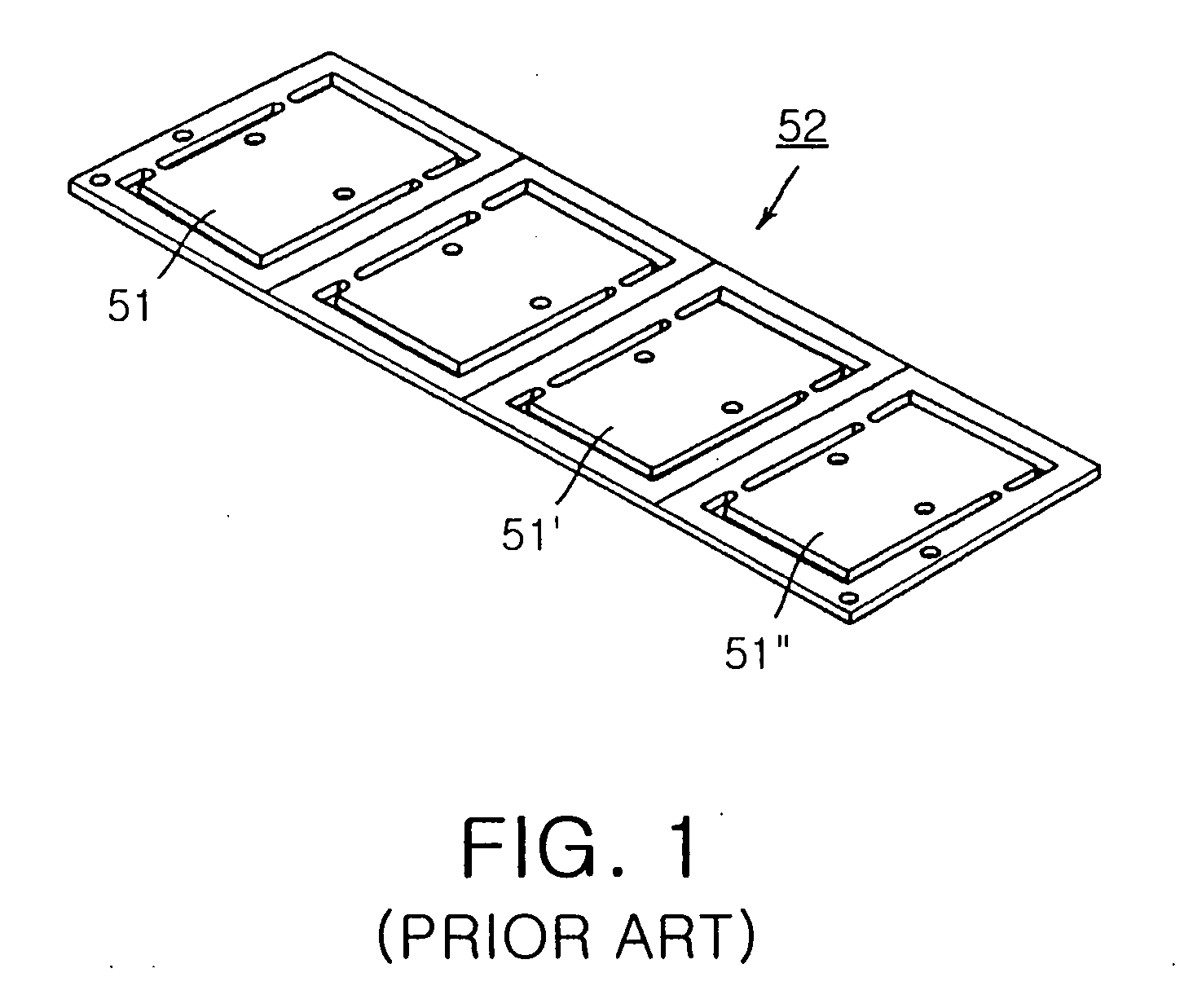
Device for coupling PCB sheet
a technology of coupling device and printed paper, which is applied in the direction of electrical apparatus casing/cabinet/drawer, manufacturing tools, instruments, etc., can solve the problems of increasing production cost and high material loss, and achieve the effects of reducing production cost, increasing product yield, and simple manner
- Summary
- Abstract
- Description
- Claims
- Application Information
AI Technical Summary
Benefits of technology
Problems solved by technology
Method used
Image

Examples
second embodiment
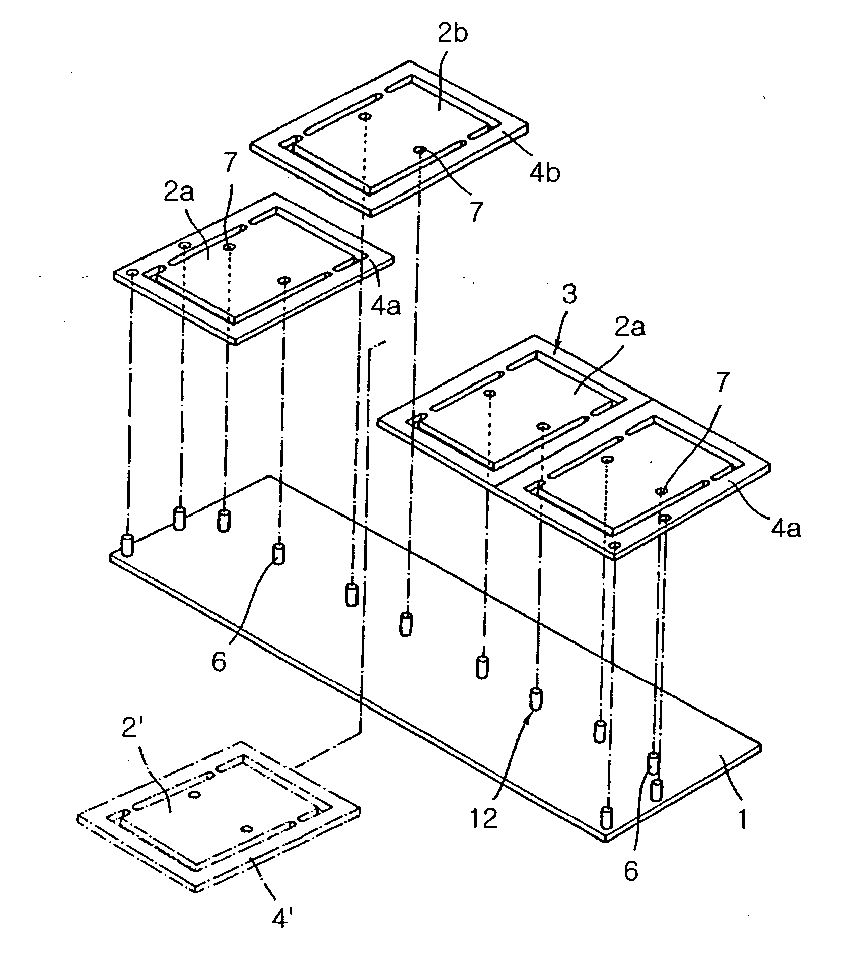
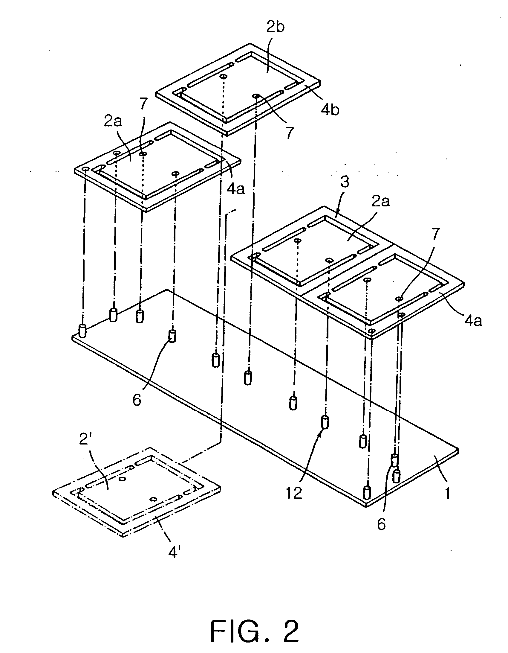
[0047]FIGS. 6 and 7 illustrate a state in which the second PCB sheet is inserted into the first PCB sheet, and the two sheets are fixed onto the PCB securing plate, in the present invention. FIG. 8 illustrates in detail the coupling portion of the first and second PCB sheets according to the present invention.
[0048] If any one of continuously printed circuit pattern parts 102 (printed on a first PCB sheet 104) is found to be a defective circuit pattern part 102′, then the rectangular portion of the defective circuit pattern part 102′ which is defined by a separation groove K is cut off by using a router or the like to form a blanked space S. Then a second PCB sheet 104′ with a new good-quality circuit pattern 102 printed thereon is placed into the rectangular space S, and then, the first and second PCB sheets 104 and 104′ are located by using a PCB securing means 110.
[0049] The first and second PCB sheets 104 and 104′ are installed on the PCB securing plate 101 by using a PCB secur...
first embodiment
[0052] A cover part 10 is put on the first and second PCB sheets 104 and 104′ which are secured on the PCB securing plate 101 like in the Thus the circuit pattern part 102 of the first and second PCB sheets 104 and 104′ are protected from the heat. The adhesive 108 is injected into the channel 109, and the injected adhesive 108 is exposed to the outside so as to be cured. In this manner, the first and second PCB sheets 104 and 104′ are coupled together.
[0053] Accordingly, as shown in FIGS. 6 to 9, if any one of the circuit pattern parts 102 of the PCB sheet 103 is found be a defective circuit pattern part 102′, then the defective circuit pattern part 102′ is cut away along the groove K to form a blanked space S like in the first embodiment. Then a second PCB sheet 104′ on which a good quality circuit pattern part 102 is printed is placed into the blanked space S, and then, the second PCB sheet 104′ is coupled to the first PCB sheet 104.
[0054] Under this condition, the reason why t...
fourth embodiment
[0067]FIGS. 14 and 15 illustrate a state in which a good quality PCB sheet is inserted into the whole PCB sheet, and the two sheets are fixed onto the PCB securing plate by using a securing jig, in the present invention. FIG. 16 is a plan view showing the coupling of a new good quality PCB sheet to the whole PCB sheet of FIG. 15.
[0068] A PCB 303 consists of a plurality of circuit pattern parts 302a which are connected to each other by connecting parts 301. If a defective circuit pattern part is found among the plurality of the circuit pattern parts 302a upon carrying out a testing, then the defective circuit pattern part is removed by cutting a connecting part 301′. In the place of the removed defective circuit pattern part, there is placed a good quality circuit pattern part 302b by means of a PCB securing means 311 into a PCB securing jig 310 which has a plurality of separating walls 315.
[0069] As shown in FIG. 16, the good quality circuit pattern part 302b has to be secured in t...
PUM
| Property | Measurement | Unit |
|---|---|---|
| width | aaaaa | aaaaa |
| temperature | aaaaa | aaaaa |
| separation distance | aaaaa | aaaaa |
Abstract
Description
Claims
Application Information
 - R&D
- Intellectual Property
- Life Sciences
- Materials
- Tech Scout
- Unparalleled Data Quality
- Higher Quality Content
- 60% Fewer Hallucinations
Browse by: Latest US Patents, China's latest patents, Technical Efficacy Thesaurus, Application Domain, Technology Topic, Popular Technical Reports.
© 2025 PatSnap. All rights reserved.Legal|Privacy policy|Modern Slavery Act Transparency Statement|Sitemap|About US| Contact US: help@patsnap.com