Logic circuit

Inactive Publication Date: 2005-06-23
INFINEON TECH AG
View PDF8 Cites 7 Cited by
  • Summary
  • Abstract
  • Description
  • Claims
  • Application Information

AI Technical Summary

Benefits of technology

[0012] In accordance with a second aspect, the invention provides a logic circuit, having: an input for one or several input operands; an output for a result or an inverted result; a first circuit branch with a first logic assembly, which is coupled to the input and the output to calculate the result; a second circuit branch with a second logic assembly, which is coupled to the input and the output to calculate the inverted result; wherein the first logic assembly and the second logic assembly have different power consumptions for calculating the result and the inverted result, respectively; and a compensation circuit in the first and/or second circuit branch to decrease a difference of the power consumption of the first and the second circuit branch.
[0013] The present invention is based on the knowledge that the security of circuits, such as particularly cryptographic circuits, such as in chip cards or SIM cards, against hardware attacks, such as power and timing attacks, can be increased when these circuits are constructed of logic circuits, where the circuit branch with the logic assembly for the calculation of the result and the circuit branch with the logic assembly for calculating the inverted result are equalized and homogenized, respectively, with regard to their run times and power consumption, respectively, by providing a delay circuit or compensation circuit in one or both of the circuit branches, which decreases the difference of the power consumptio

Problems solved by technology

It is a disadvantage of the logic device described with reference to FIG. 4 that when using such logic devices in cryptographical circuits, such as chip cards or SIM cards, different run times and power consumption are caused, depending on the data to be encrypted within a logic device according to FIG. 4, which, in turn, present a potential for possi

Method used


Image

  • Logic circuit
  • Logic circuit
  • Logic circuit

Examples


Embodiment Construction

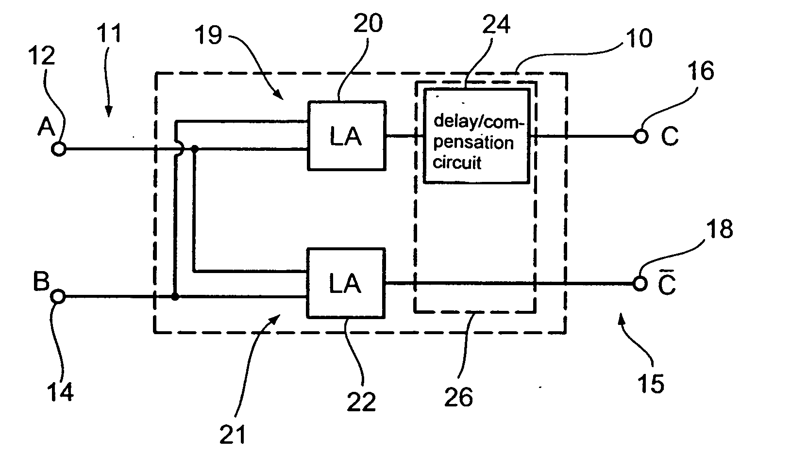
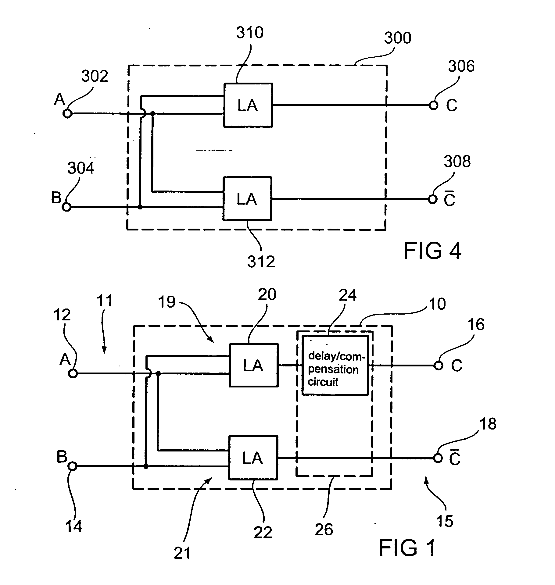
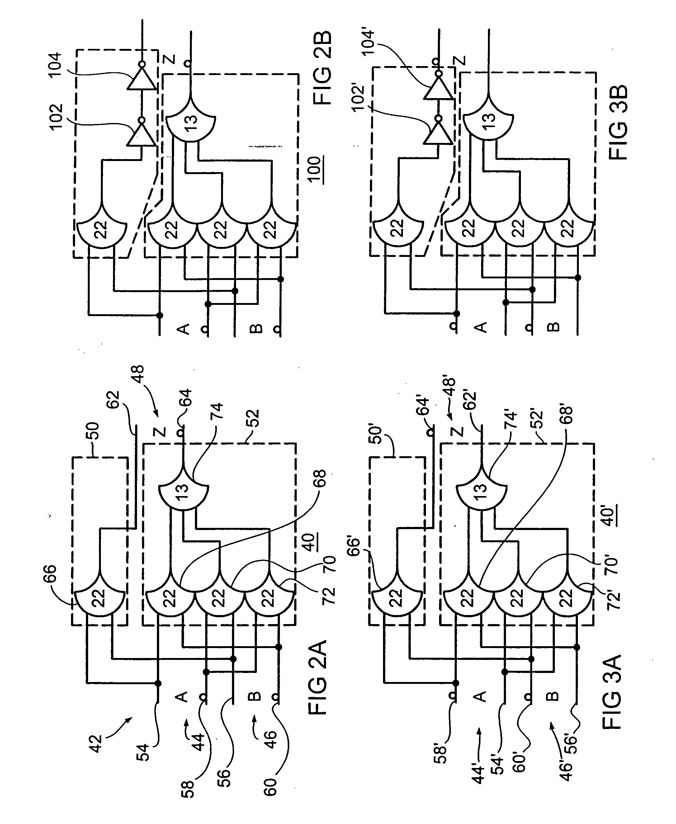
[0022] It should be noted that the same or functionally equal elements are indicated with the same or similar reference numbers in FIGS. 2 and 3, and that a repeated description of these elements is omitted in the following description of these Figures.

[0023] First, a logic circuit according to a general embodiment of the present invention is described with reference to FIG. 1, where the logic circuit, like the one of FIG. 4, maps two input operands A, B to a result operand C, and outputs a result C and an inverted result {overscore (C)}. The logic circuit of FIG. 1, which is generally indicated with 10, comprises an input 11 with an operand input 12 for the input operand A and an operand input 14 for the input operand B on the input side, an output 15 with a partial output or sub output 16 for the result C and a partial output 18 for the inverted result {overscore (C)} on the output side, as well as in-between a circuit branch 19 coupled to the input 11 and the partial output 16, ...


PUM


Abstract

A logic circuit includes an input for one or several input operands, an output for a result and an inverted result, a first circuit branch with a first logic assembly, which is coupled to the input and the output, to calculate the result, as well as a second circuit branch with a second logic assembly, which is coupled to the input and the output, to calculate the inverted result, wherein the first logic assembly and the second logic assembly have different run times for calculating the result and the inverted result, respectively. Further, a delay circuit and a compensation circuit, respectively, are provided in the first and/or second circuit branch to reduce a difference of the run times and the power consumptions, respectively, of the first and the second circuit branch.

Description

CROSS-REFERENCE TO RELATED APPLICATION [0001] This application is a continuation of copending International Application No. PCT / EP2003 / 006260, filed Jun. 13, 2003, which designated the United States, and was not published in English and is incorporated herein by reference in its entirety.BACKGROUND OF THE INVENTION [0002] 1. Field of the Invention [0003] The present invention relates generally to logic circuits and particularly to such logic circuits where two different circuit branches are connected between input and output to calculate a result and an inverted result in dependency on one or several inputs. [0004] 2. Description of Prior Art [0005] Circuits of this type are used, for example, in circuits with a dual rail encoding or in circuits of the NCL (Null Convention Logic® (registered trademark)) of the company Theseus or in different circuits. [0006]FIG. 4 generally shows the structure of such logic circuits based on an example of a logic device, which maps two input operand...

Claims


Application Information

Patent Timeline
IPC IPC(8): H03K5/151H03K19/003
CPCH03K19/00323H03K5/151
Inventor BOCK, HOLGER
Owner INFINEON TECH AG
Why Eureka
Try Eureka