Multi-chip assembly and method for driving the same

a multi-chip assembly and assembly technology, applied in the direction of basic electric elements, bedpans, transportation and packaging, etc., can solve the problem that the electronic appliances equipped with the conventional multi-chip assembly cannot be easily operated, and achieve the effect of flexible installation

Inactive Publication Date: 2005-07-14
SK HYNIX INC
View PDF6 Cites 5 Cited by
  • Summary
  • Abstract
  • Description
  • Claims
  • Application Information

AI Technical Summary

Benefits of technology

[0018] According to the present invention, it is possible to provide the multi-chip assembly in the form of a package fabricated by stacking chips designed with mutually different devices driven through a single power source. Therefore, the multi-chip assembly of the present invention allows electronic appliance to have compactness, slimness and lightness sizes. In particular, the multi-chip assembly of the present invention can be flexibly installed in various electronic appliances.

Problems solved by technology

For this reason, if an electronic appliance is equipped with the conventional multi-chip assembly having chips designed with mutually different devices, a problem may occur because the electronic appliance requires a plurality of power sources for applying power to the devices.
Accordingly, although the conventional multi-chip assembly may allow the electronic appliance to be fabricated with a lightness, slimness, and compactness structure while simplifying assembling processes thereof, the electronic appliance equipped with the conventional multi-chip assembly cannot be easily operated.

Method used


Image

  • Multi-chip assembly and method for driving the same
  • Multi-chip assembly and method for driving the same
  • Multi-chip assembly and method for driving the same

Examples


Embodiment Construction

[0025] Hereinafter, the present invention will be described in detail.

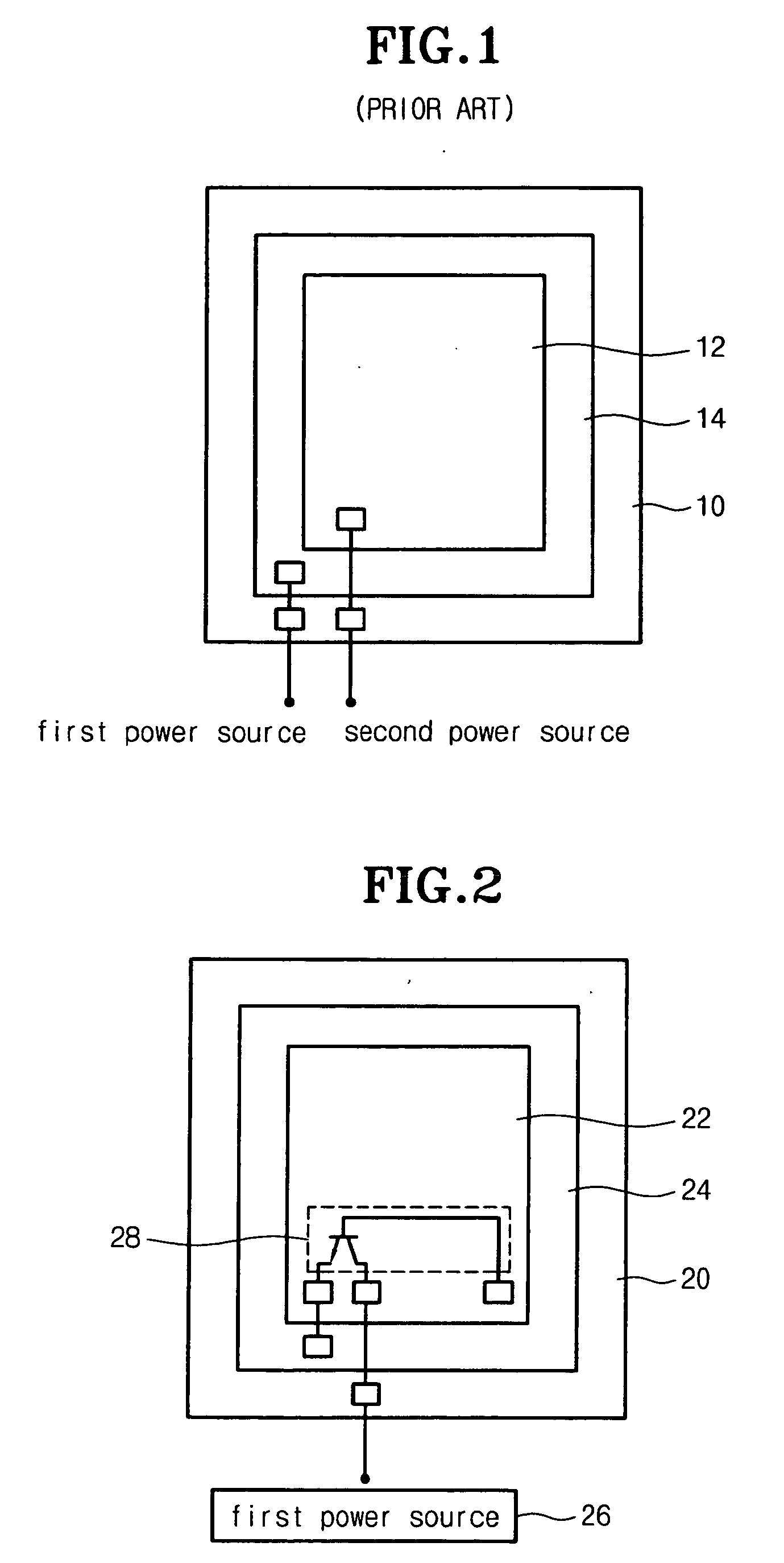
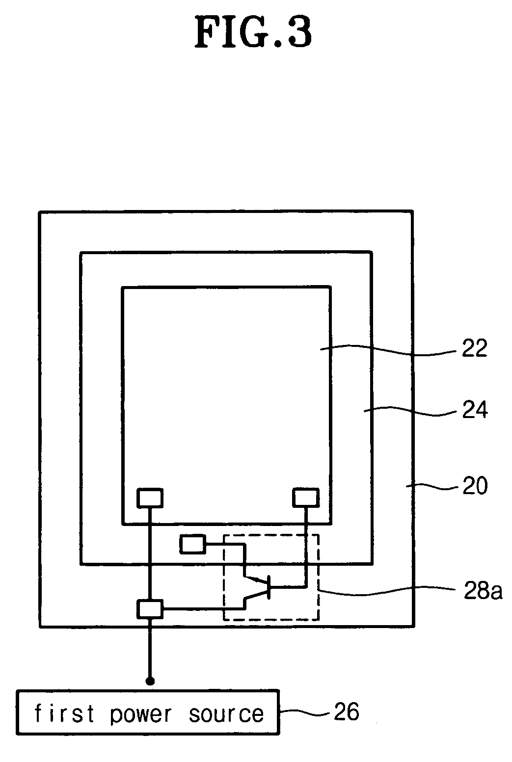
[0026] A first chip is designed with a first device driven by a first power source. The first chip includes an SRAM device, which is driven by a power source capable of applying voltages of 2.5 to 3.5V to the SRAM device. Preferably, the SRAM device is driven by a power source applying voltages of 3V to the SRAM device. In addition, a second chip is designed with a second device driven by a second power source. The second chip includes a flash memory device, which is driven by a power source capable of applying voltages of 1.6 to 2.0V to the flash memory device. Preferably, the flash memory device is driven by a power source applying voltages of 1.8V to the flash memory device.

[0027] In addition, the multi-chip assembly includes a printed circuit board and first and second chips mounted on the printed circuit board. Preferably, the first chip is stacked on the second chip. However, it is also possible to stack t...


PUM


Abstract

Disclosed are a multi-chip assembly and a method for driving the same. The multi-chip assembly includes a first chip designed with a first device driven by a first power source and a second chip designed with a second device driven by a second power source. A power applying section applies first power to the first device of the first chip and a power converting section converts the first power to second power upon receiving the first power from the power applying section and applies the second power to the second device of the second chip. It is possible to provide the multi-chip assembly in the form of a package fabricated by stacking chips designed with mutually different devices driven through a single power source.

Description

BACKGROUND OF THE INVENTION [0001] 1. Field of the Invention [0002] The present invention relates to a multi-chip assembly and a method for driving the same, and more particularly to a stack-type multi-chip assembly and a method for driving the same. [0003] 2. Description of the Prior Art [0004] Recently, designs of electronic appliances have tended toward lightness, slimness, and compactness. Therefore, it is important to provide a high-density semiconductor chip package having a lightness, slimness, and compactness structure. To this end, semiconductor packages have been developed in the form of multi-chip assemblies, in which at least two chips are horizontally stacked. [0005] In general, a semiconductor package in the form of a multi-chip assembly is used for receiving chips designed with the same device. Currently, the multi-chip assembly has been developed such that it can receive chips designed with mutually different devices. Accordingly, the multi-chip assembly may allow el...

Claims


Application Information

Patent Timeline
Patent Type & Authority Applications(United States)
IPC IPC(8): H01L21/82H01L23/12H01L23/52H01L25/00H01L25/18H01L27/00
CPCH01L25/18H01L2924/0002H01L2924/00A61G9/003A61G2200/32A61G2200/34A61G2203/12A61G2203/30
Inventor KIM, KWI WOOKLEE, CHANG YEOL
Owner SK HYNIX INC
Why Eureka
Try Eureka