At least penta-sided-channel type of FinFET transistor

a finfet transistor, penta-sided channel technology, applied in transistors, electrical devices, semiconductor devices, etc., can solve the problems of short channel effect, need to reduce transistor size, and create problems

Active Publication Date: 2005-07-21
SAMSUNG ELECTRONICS CO LTD
View PDF15 Cites 237 Cited by
  • Summary
  • Abstract
  • Description
  • Claims
  • Application Information

AI Technical Summary

Problems solved by technology

The need to reduce transistor size is a perennial problem to be solved in the art of integrated circuits.
But then a minimum channel length (relative to other physical parameters of the transistor) was achieved below which problems were created, e.g., short channel effects.
This lowers a threshold voltage for the corners relative to the sides, leading to higher current flow at the corners and generally non-uniform performance of the FinFET.
Despite many attempts, the Background Art has not been able to develop a technique to remove material from square corners of triple-gate FinFET 700 (or a double-gate version thereof) that does not irreparably damage the remaining portion of fin 702b or result in a non-uniform width thereof.

Method used


Image

  • At least penta-sided-channel type of FinFET transistor
  • At least penta-sided-channel type of FinFET transistor
  • At least penta-sided-channel type of FinFET transistor

Examples


Embodiment Construction

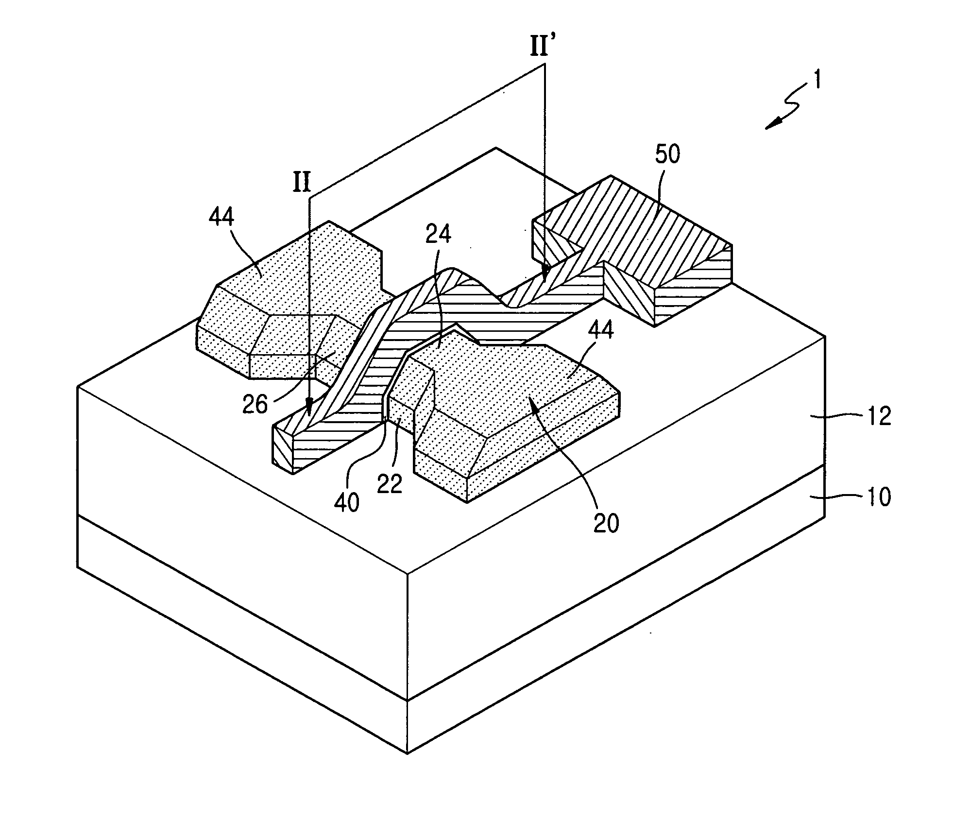
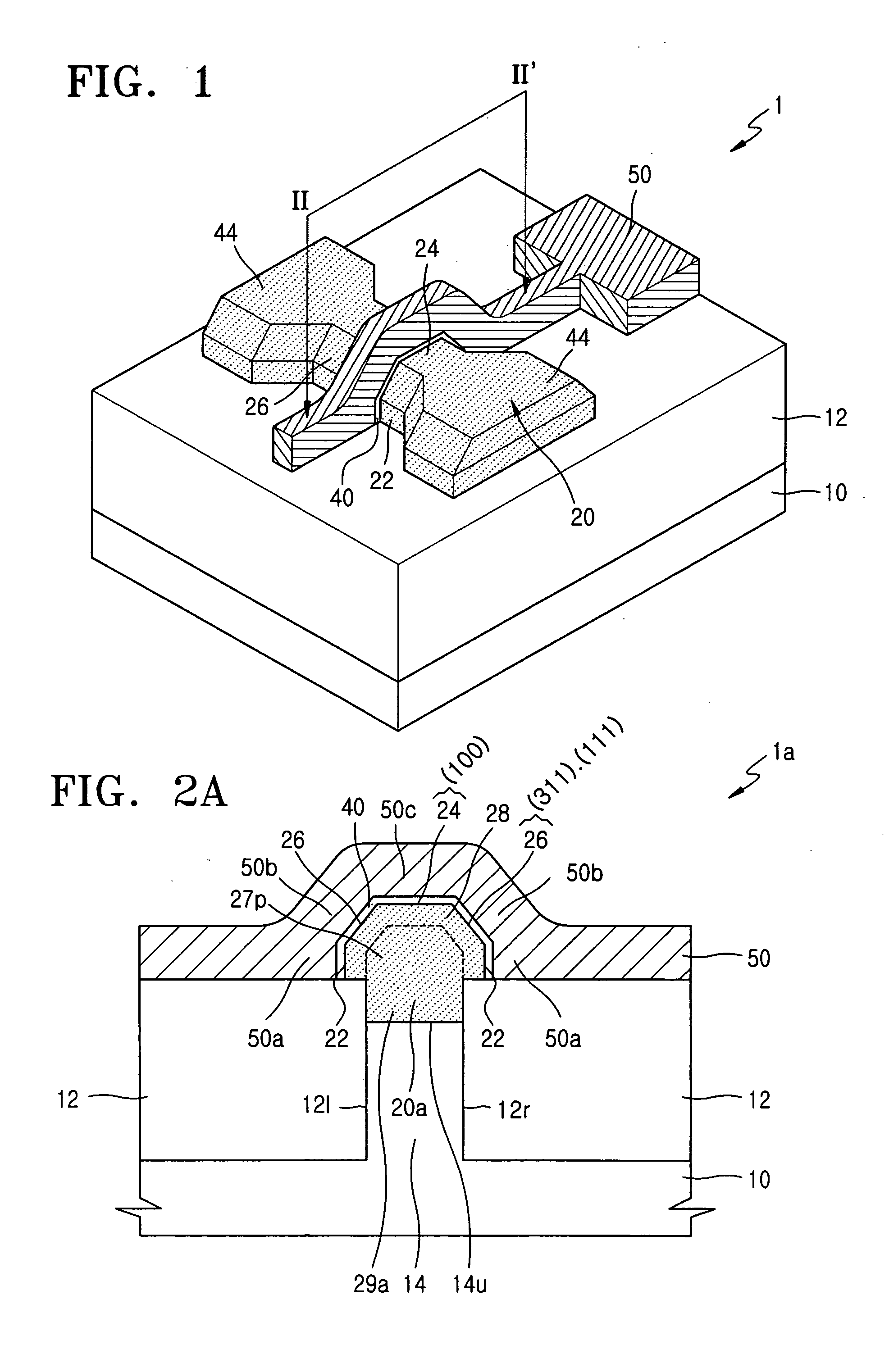
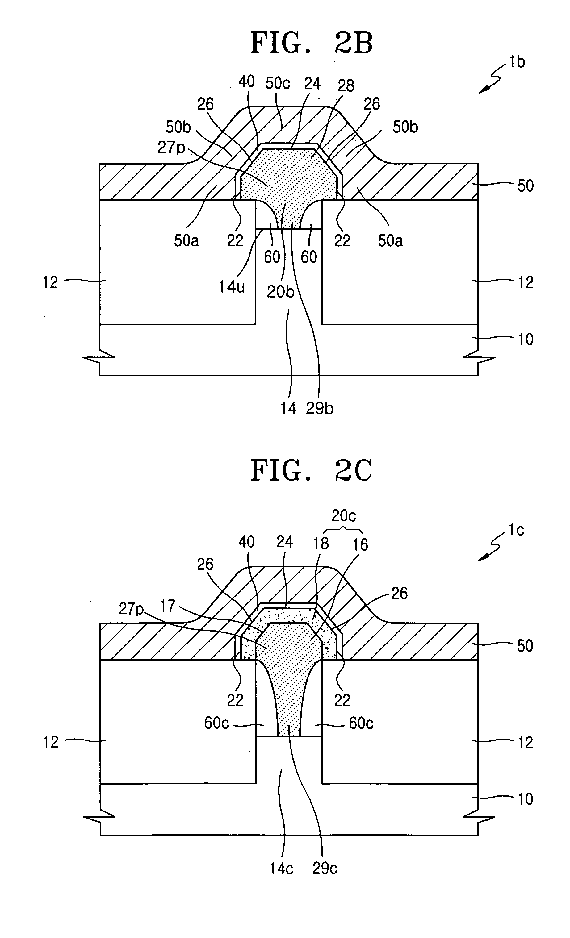
[0025] In developing the present invention, the following problem with the Background Art was recognized and a path to a solution identified. The Background Art assumes that mitigation (by rounded-corner approximation) of the problematic corner effect (again, caused by substantially square corners of the fin-shaped channel) of a Background Art FinFET can only be accomplished subtractively by removing material representing the substantially square portion of the corners. It is now recognized that an obtuse angle significantly larger than 90° can significantly reduce the corner effect. Such an obtuse angle approximates the rounding of corners, but can be achieved additively by growing the fin rather than subtractively by removing material from a fin having substantially square corners. For example, epitaxial growth of silicon can achieve the desired approximation of a rounded-corner fin without the negative consequential effects upon other aspects of the inchoate FinFET that are conse...


PUM


Abstract

An at least penta-sided-channel type of FinFET transistor may include: a base; a semiconductor body formed on the base, the body being arranged in a long dimension to have source / drain regions sandwiching a channel region, at least the channel, in cross-section transverse to the long dimension, having at least five planar surfaces above the base; a gate insulator on the channel region of the body; and a gate electrode formed on the gate insulator.

Description

CROSS-REFERENCE TO RELATED APPLICATIONS [0001] This U.S. non-provisional patent application claims priority under 35 U.S.C. § 119 of Korean Patent Application 2004-3568 filed on Jan. 17, 2004, the entire contents of which are hereby incorporated by reference. BACKGROUND OF THE PRESENT INVENTION [0002] The need to reduce transistor size is a perennial problem to be solved in the art of integrated circuits. One way that the Background Art reduced transistor size was to reduce the length of the channel. Doing so effectively reduced the overall footprint of the transistor. But then a minimum channel length (relative to other physical parameters of the transistor) was achieved below which problems were created, e.g., short channel effects. [0003] The Background Art responded by developing a transistor architecture that reduced the transistor's footprint size while maintaining at least the minimum channel length. The solution can be explained via analogy to an inchworm. FIGS. 5A-5B are si...

Claims


Application Information

Patent Timeline
Patent Type & Authority Applications(United States)
IPC IPC(8): H01L21/336H01L29/78H01L29/786
CPCH01L29/7853H01L29/66795
Inventor RHEE, HWA-SUNGKIM, HYUN-SUKTETSUJI, UENOYOO, JAE-YOONLEE, SEUNG-HWANLEE, HOPARK, MOON-HAN
Owner SAMSUNG ELECTRONICS CO LTD
Why Eureka
Try Eureka