Critical pattern extracting method, critical pattern extracting program, and method of manufacturing semiconductor device

a critical pattern and extracting method technology, applied in the direction of photomechanical treatment originals, instruments, photomechanical equipment, etc., can solve the problems of deterioration of performance, increase of edge roughness caused by shortage of resist film thickness in processing, and decrease of operation speed of semiconductor devices

Inactive Publication Date: 2005-07-28
KK TOSHIBA
View PDF7 Cites 9 Cited by
  • Summary
  • Abstract
  • Description
  • Claims
  • Application Information

AI Technical Summary

Problems solved by technology

A few shortage of thickness of a resist film, which does not cause any problem in manufacturing processes for semiconductor devices having a large feature size, causes a problem in processing of an underlying film having a small feature size.
In a serious situation, there is a phenomenon in which edge roughness caused by a shortage of thickness of the resist film in processing increases.
At least one of the variation in dimension and the increase in edge roughness causes deterioration of performance such as a decrease in operation speed of a semiconductor device or an increase in required power in, e.g., a gate structure.
In addition, the edge roughness in an element isolation pattern causes an increase in leak current caused by defective burying of an insulating film.
For this reason, correction accuracy of a mask pattern cannot be fundamentally improved.

Method used


Image

  • Critical pattern extracting method, critical pattern extracting program, and method of manufacturing semiconductor device
  • Critical pattern extracting method, critical pattern extracting program, and method of manufacturing semiconductor device
  • Critical pattern extracting method, critical pattern extracting program, and method of manufacturing semiconductor device

Examples


first embodiment

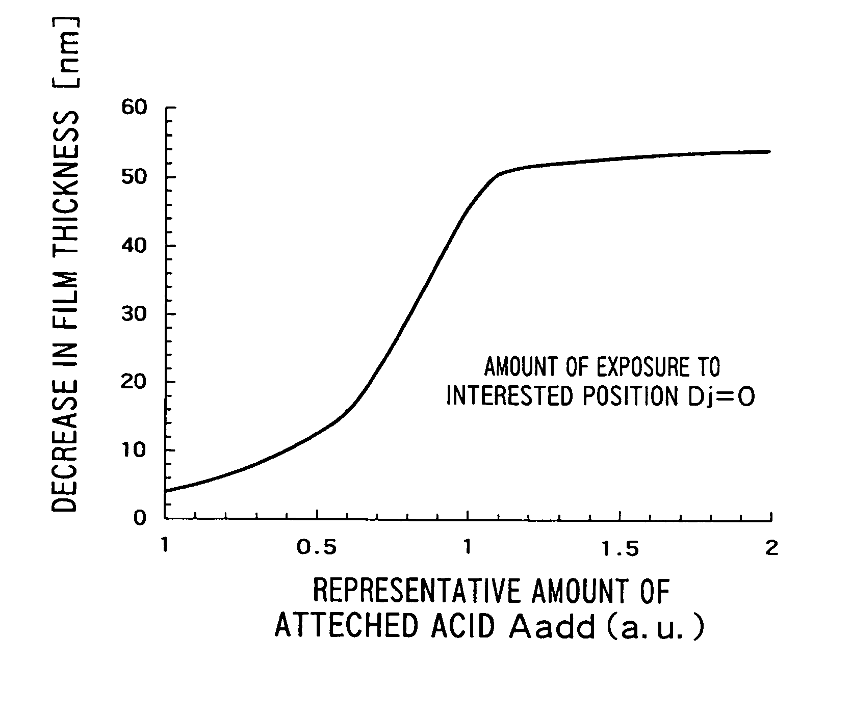
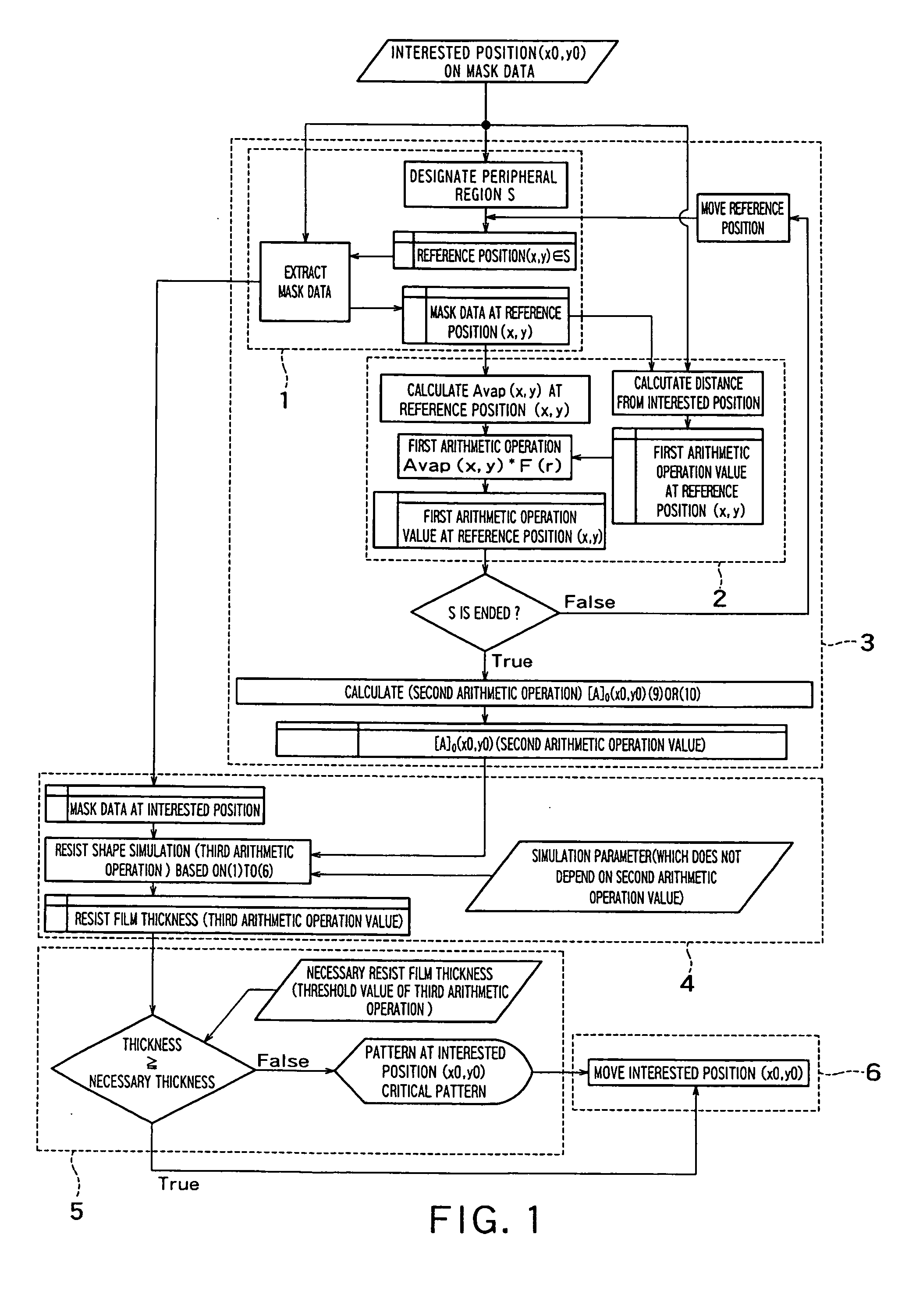
[0034] As a characteristic feature of the embodiment, an amount of acids vapored from a periphery of an interested resist film during PEB (Post Exposure Bake) is used to calculate a concentration of acids in a vapor immediately above the interested resist film or a representative value of the concentration by simulation. Simulation is performed by using the calculated acid concentration to calculate a decrease in thickness of the interested resist film after development, and the calculated decrease in film thickness is compared with a threshold value. In this manner, it is decided whether a mask data portion corresponding to the interested resist film corresponds to a critical pattern or not.

[0035] In this case, the critical pattern is a pattern in mask data which constitutes barriers to realization of a desired function of a semiconductor device. More specifically, the critical pattern is a pattern in mask data which may induce a circuit malfunction. In this point, the critical pa...

second embodiment

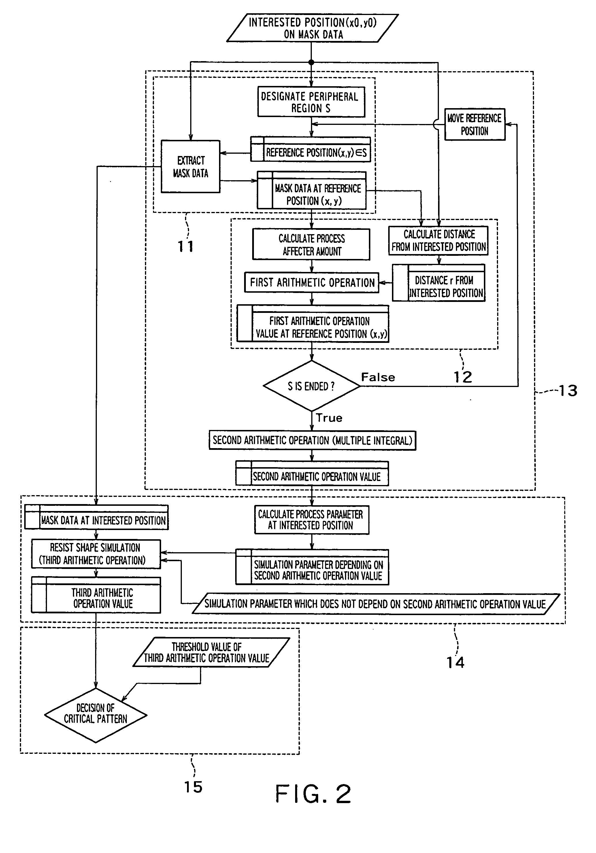
[0093] In the first embodiment, in the case where the base amount B0 is sufficiently small, a term of B0 in (Equation 10) is separated to make it possible to change (Equation 10) into (Equation 11). In this equation, G denotes a constant.

[A]0(x0, y0)≈h′∫∫exp{1−C×Ei×I(x,y))}·F(r)dxdy−G  (Equation 11)

[0094] In this (Equation 11), values h′, F(r), and G may be calculated by at least one of an experiment method and an analytic method.

[0095] (Equation 11) has a form which is simpler than that of (Equation 9). Therefore, a calculation time in the second embodiment can be made shorter than that in the first embodiment.

third embodiment

[0096] In the first embodiment, an amount of acids [A](t=0) (see (Equation 1)) generated from PAG by exposure to a position (x,y,z) on a resist film can be approximated to as in (Equation 12) in a region given by C×E×I(x,y,z)<<1.

[A](t=0)≈C×Ei×I(x,y,z)  (Equation 12)

[0097] In the case where the approximation of (Equation 12) is applied to (Equation 11), and if an electric field intensity in the direction of thickness of the resist film is uniformly (I(x,y,z)=I(x,y)), the following (Equation 13) is derived.

[A]0(x0,y0)≈h′∫∫C×Ei×I(x, y)·F(r)dxdy−G  (Equation 13)

[0098] As is apparent from (Equation 13), the acid concentration [A]0 (x0,y0) on the resist film at the interested position (x0,y0) is in proportion to an amount of light absorption (Ei×I(x,y)) in the resist film at the reference position (x,y) or an electric field intensity (I(x,y)) in the resist film at the reference position (x,y). Therefore, in order to calculate the thickness of the resist film at the interested position...


PUM

PropertyMeasurementUnit
thicknessaaaaaaaaaa
thicknessaaaaaaaaaa
distanceaaaaaaaaaa

Abstract

According to a aspect of the present invention, there is provided a critical pattern extracting method which extracts critical patterns from mask data for manufacturing a photomask used in a lithography step, comprising at least: extracting mask data of a peripheral region within a predetermined range from an interested portion to be decided in the mask data; defining portions constituting the peripheral region as reference portions and calculating process generation amounts generated from the each reference portion in the lithography step by simulation; performing a predetermined arithmetic operation by using the process generation amounts and distances between the interested portion and the each reference portion; performing multiple integral of an arithmetic operation value obtained by the predetermined arithmetic operation in the peripheral region or an arithmetic operation equivalent to the multiple integral to calculate a process affecter amount; and comparing the process affecter amount with a predetermined threshold value.

Description

CROSS REFERENCE TO RELATED APPLICATIONS [0001] This application claims the benefit of priority under 35USC § 119 to Japanese Patent Application No. 2003-409015 filed on Dec. 8, 2003, the entire contents of which are incorporated herein by reference. BACKGROUND OF THE INVENTION [0002] 1. Field of the Invention [0003] The present invention relates to a critical pattern extracting method and program which extracts a critical pattern from mask data of a photomask used in lithography process in manufacturing a semiconductor device, a magnetic device, or the like, and a method of manufacturing a device. [0004] 2. Related Art [0005] As a film thickness of a resist film used in lithography, an aspect ratio of 3 or less is generally used to secure an process margin against deterioration of resolution and pattern collapse caused by shrinkage of feature size of a circuit pattern. For example, in the case where the minimum line width in lithography is 90 nm, the resist film having a film thickn...

Claims


Application Information

Patent Timeline
Patent Type & Authority Applications(United States)
IPC IPC(8): G03F1/36G03F1/68G03F1/70G03F7/00G03F9/00G06F17/50H01L21/027
CPCG03F1/36G03F1/144
Inventor KAWAMURA, DAISUKENOJIMA, SHIGEKIMIMOTOGI, SHOJI
Owner KK TOSHIBA
Why Eureka
Try Eureka