Method of making microelectronic packages including electrically and/or thermally conductive element

a technology of electrical and/or thermal conductivity elements and microelectronic components, which is applied in the direction of semiconductor devices, semiconductor/solid-state device details, electrical apparatus, etc., can solve the problems of time-consuming and expensive semiconductor chips with each other

Inactive Publication Date: 2005-08-04
TESSERA INC
View PDF2 Cites 18 Cited by
  • Summary
  • Abstract
  • Description
  • Claims
  • Application Information

AI Technical Summary

Benefits of technology

[0014] Amicroelectronic element is disposed within the space. An encapsulant includes an interior portion at least partially filling the space and at least partially surrounding the microelectronic element, and an exterior portion being disposed outside of said interior space in contact with the conductive element, said portions of said encapsulant being connected to one another through said one or more openings in the conductive element. Stated another way, in this aspect of the invention, portions of the encapsulant are exposed at the exterior of the assembly, desirably along the side walls of the conductive element. For example, where the conductive element includes multiple pillars defining the side walls, portions of the encapsulant fill the gaps in the side walls so that these portions are exposed at the outside of the assembly. Thus, even where the conductive element does not provide a complete, continuous covering over the microelectronic element, the encapsulant fills the gaps. The encapsulant exposed at the exterior of the assembly may also serve to protect the conductive element from mechanical damage.

Problems solved by technology

Assembling such individual elements, commonly known as “cans”, with each semiconductor chip is costly and time-consuming.

Method used


Image

  • Method of making microelectronic packages including electrically and/or thermally conductive element
  • Method of making microelectronic packages including electrically and/or thermally conductive element
  • Method of making microelectronic packages including electrically and/or thermally conductive element

Examples


Embodiment Construction

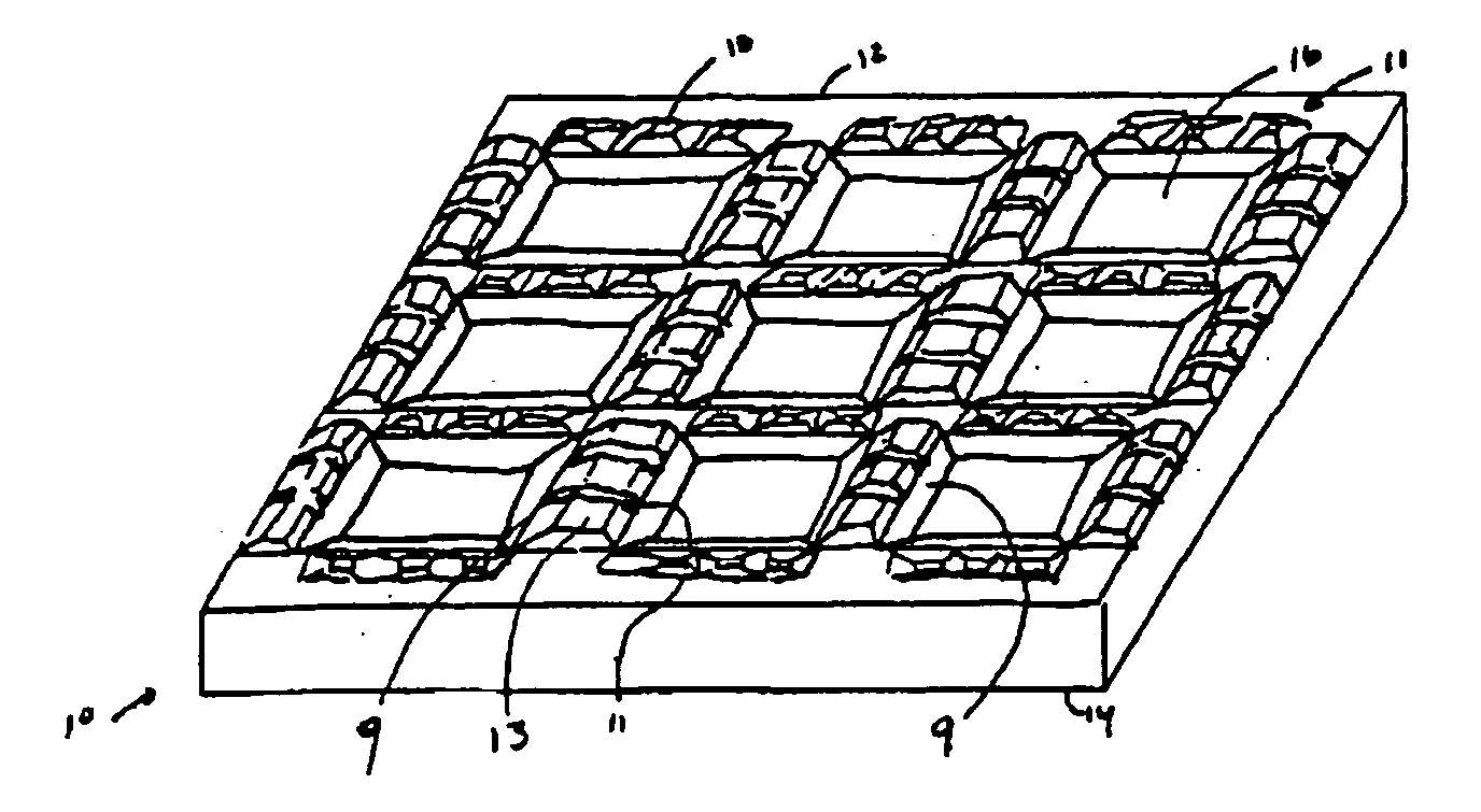
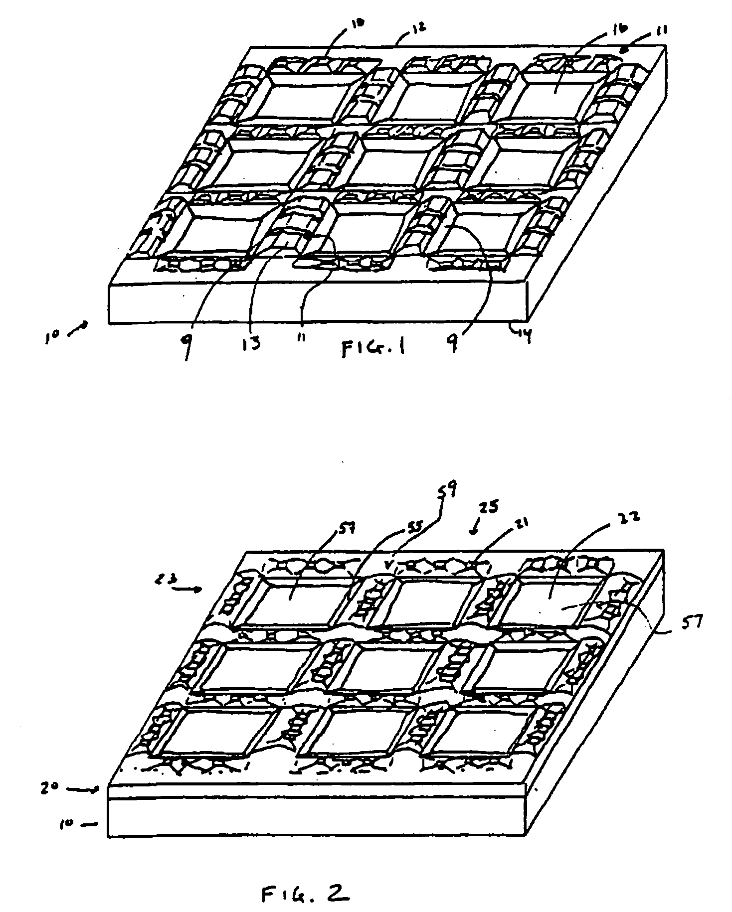
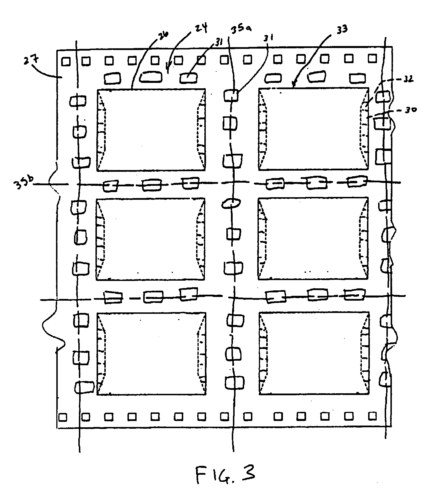
[0031] A method in accordance with one embodiment of the invention includes using a support 10. Support 10 comprises an element having a first major surface 12 and a second major surface 14 facing oppositely from the first major surface 12. Recesses 16 are formed in the first major surface 12 of the support 10. The support has surface portions 11 surrounding each recess 16 and projecting upwardly from the bottom surface of the recess. In this embodiment, each surface portion 11 is in the form of a substantially continuous wall extending along one side of a recess or forming a division between two adjacent recesses. Each surface portion or wall 11 has outwardly-sloping surfaces extending from the top of the wall to the bottom surface of each adjacent recess, so that each wall widens toward the bottom of the recess whereas each recess widens toward the top or open side of the recess. Each surface portion or wall 11 has a set of spaced apart support protrusions or bumps 13 disposed alo...


PUM


Abstract

A method of manufacturing a plurality of microelectronic packages including electrically and / or thermally conductive elements. The method includes providing a support structure having a plurality of protrusions and depressions extending outwardly from the support. A conductive element is then mated to the support structure in a male-to-female relationship. The depressions formed in the support structure and conductive element are used to house a microelectronic element such as a semiconductor chip. A substrate is provided so as to cover substantially each depression located in the conductive element. Leads interconnect contacts to the chip to terminals on the substrate. A curable encapsulant material may be deposited into the depression so as to protect and support the leads and the microelectronic element. Additionally, the curable encapsulant material forms part of the exterior of a single resulting chip package once the assembly is diced and cut into individual packages.

Description

CROSS-REFERENCE TO RELATED APPLICATIONS [0001] This application is a divisional of U.S. patent application Ser. No. 10 / 607,289 filed Jun. 26, 2003, which claims the benefit of U.S. Provisional Application No. 60 / 391,814 filed on Jun. 27, 2002, the disclosures of which are hereby incorporated herein by reference.BACKGROUND OF THE INVENTION [0002] The present invention relates to methods of making microelectronic assemblies, such as semiconductor chip packages, including an electrically and / or thermally conductive element. [0003] Modern electronic devices utilize semiconductor chips, commonly referred to as “integrated circuits”, which incorporate numerous electronic elements. These chips are mounted on substrates that physically support the chips and electrically interconnect each chip with other elements of a circuit. The substrate may be a part of a chip package including terminals for interconnecting the chip with external circuit elements. The interconnection between the chip and...

Claims


Application Information

Patent Timeline
Patent Type & Authority Applications(United States)
IPC IPC(8): H01L21/56H01L21/68H01L23/13H01L23/24H01L23/31H01L23/367H01L23/433H01L23/492H01L23/498H01L23/552
CPCH01L21/561H01L2924/014H01L21/6835H01L23/13H01L23/24H01L23/3114H01L23/3128H01L23/3675H01L23/4334H01L23/492H01L23/49816H01L23/4985H01L23/552H01L24/26H01L24/83H01L24/97H01L2224/48091H01L2224/48227H01L2224/73153H01L2224/8319H01L2224/83801H01L2224/97H01L2225/0651H01L2225/0652H01L2225/06582H01L2225/06589H01L2924/01005H01L2924/01029H01L2924/01042H01L2924/01079H01L2924/01082H01L2924/14H01L2924/16152H01L2924/3025H01L21/565H01L2924/01033H01L2924/01024H01L2924/01006H01L24/48H01L2924/00014H01L2224/83H01L2924/12042H01L2924/181H01L2224/05599H01L2224/45099H01L2224/85399H01L2924/00H01L2924/00012H01L2224/45015H01L2924/207
Inventor BEROZ, MASUDKONG, BOB WEN ZHONGWARNER, MICHAEL
Owner TESSERA INC
Why Eureka
Try Eureka