PAA- based etchant, methods of using same, and resultant structures

a technology of etchants and etchants, applied in the field of etchants based on etchants, methods of using same, and resultant structures, can solve the problems of short channel effects, problems created, and the need to reduce transistor siz

Inactive Publication Date: 2005-08-04
SAMSUNG ELECTRONICS CO LTD
View PDF15 Cites 74 Cited by
  • Summary
  • Abstract
  • Description
  • Claims
  • Application Information

AI Technical Summary

Benefits of technology

[0013] At least one embodiment of the present invention provides a wet-etch composition. Such a wet-etch composition (hereafter, PAA-based etchant) may include: peracetic acid (PAA); and a fluorinated acid; a relative amount of the PAA in the composition being sufficient to ensure an etch rate of (P-doped-SiGe):(P-doped-Si) that is substantially the same as an etch rate of (N-doped-SiGe):(N-doped-Si). Such a wet-etch composition is hereafter referred to as a PAA-based etchant.

Problems solved by technology

The need to reduce transistor size is a perennial problem to be solved in the art of integrated circuits.
But then a minimum channel length (relative to other physical parameters of the transistor) was achieved below which problems were created, e.g., short channel effects.

Method used


Image

  • PAA- based etchant, methods of using same, and resultant structures
  • PAA- based etchant, methods of using same, and resultant structures
  • PAA- based etchant, methods of using same, and resultant structures

Examples


Embodiment Construction

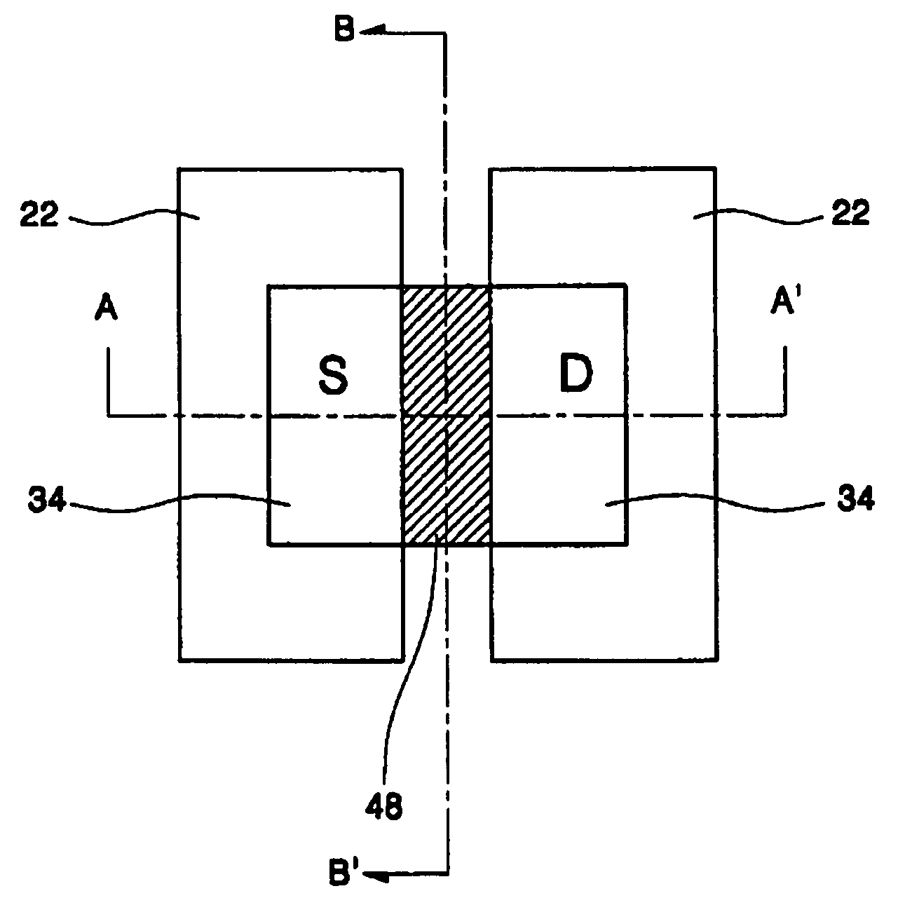
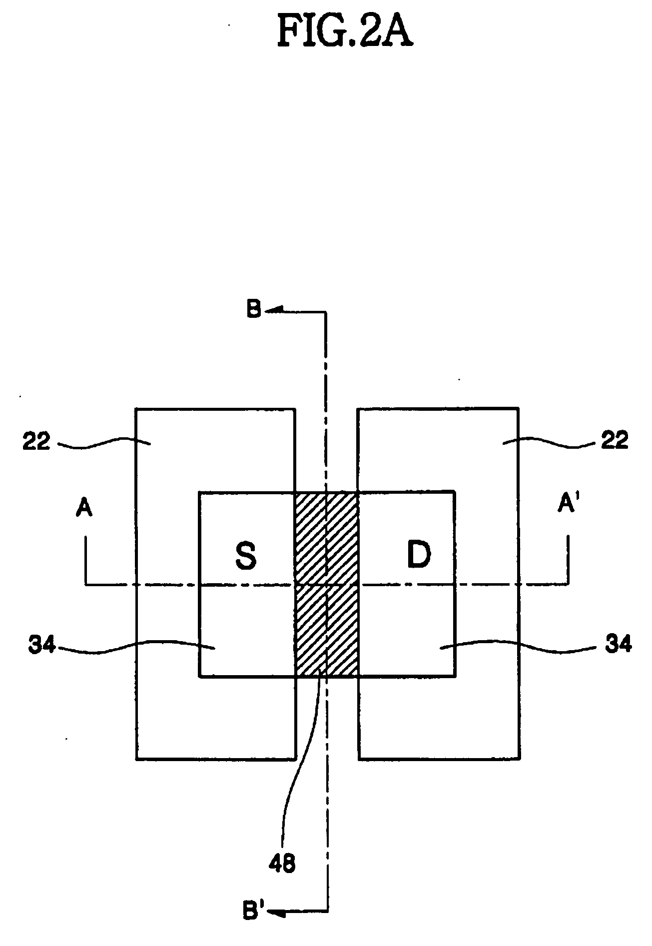
[0032] This section of the present application makes mention of FIGS. 1A-1B, 2A-2C, 3A-3R, 4A 4G, 5, 6A-6C, 7A-7L and 8, but they are not discussed in that order. Rather, they are discussed in the order 1A, 5, 6A-6C, 1B, 2A-2C, 3A-3R, 4A-4G, and 8.

[0033] In developing the present invention, the following problems with the Background Art were recognized and a path to a solution identified.

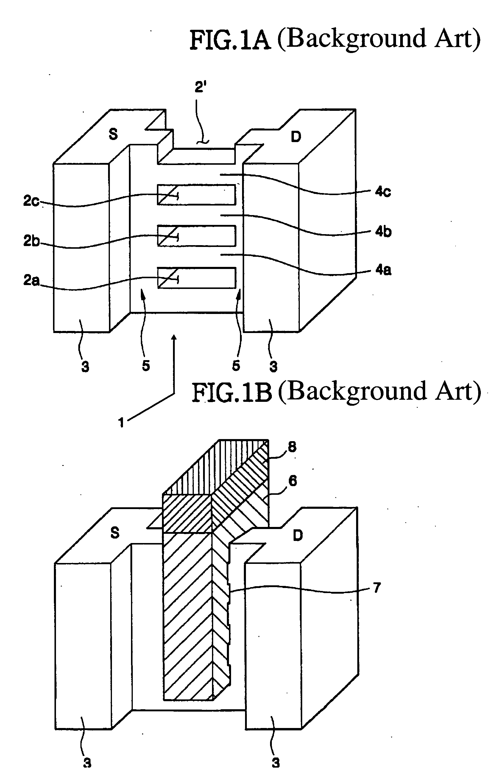
[0034] As noted, to obtain the arrangement of bridges 4a, 4b and 4c and tunnels 2a, 2b and 2c in Background Art FIG. 1A, the precursor to bridge-region 1 of the active pattern is etched with an etchant that is selective to SiGe over Si. The Background Art used one of four different etchant compositions: a first mixture of hydrofluoric acid (HF), nitric acid (HNO3) and water (H2O); a second mixture of hydrofluoric acid (HF), hydrogen peroxide (H2O2) and water (H2O); a third mixture of ammonium hydroxide (NH4OH), H2O2 and H2O; a fourth mixture of HF, HNO3, acetic acid (CH3COOH) and deionized H2O (DI...


PUM

PropertyMeasurementUnit
etch rate ratioaaaaaaaaaa
conductiveaaaaaaaaaa
doping concentrationaaaaaaaaaa

Abstract

A wet-etch composition may include: peracetic acid (PAA); and a fluorinated acid; a relative amount of the PAA in the composition being sufficient to ensure an etch rate of (P-doped-SiGe):(P-doped-Si) that is substantially the same as an etch rate of (N-doped-SiGe):(N-doped-Si). Such a wet-etch composition is hereafter referred to as a PAA-based etchant and can be used to make, e.g., a CMOS MBCFET, an electrode of a capacitor, etc.

Description

CONTINUITY AND PRIORITY [0001] This application is a continuation-in-part of two copending U.S. patent applications: one having Ser. No. 10 / 610,607, filed Jul. 1, 2003, for which priority is claimed under 35 U.S.C. §120, and the disclosure of which is incorporated herein in its entirety; and the other having Attorney Docket No. “MJM Do. No. 9898-313”, filed Apr. 28, 2004 (itself claiming foreign priority upon Korean patent application No. P2003-0057009 filed Aug. 13, 2003), for which priority is claimed under 35 U.S.C. §120, and the disclosure of which is incorporated herein in its entirety.BACKGROUND OF THE PRESENT INVENTION [0002] The need to reduce transistor size is a perennial problem to be solved in the art of integrated circuits. One way that the Background Art reduced transistor size was to reduce the length of the channel. Doing so effectively reduced the overall footprint of the transistor. But then a minimum channel length (relative to other physical parameters of the tra...

Claims


Application Information

Patent Timeline
Patent Type & Authority Applications(United States)
IPC IPC(8): C09K13/08H01L21/308C23F1/24G11C8/02H01L21/306H01L21/3213H01L21/336H01L21/8238H01L21/8242H01L27/108H01L29/786
CPCC09K13/08H01L29/78696H01L21/32134H01L21/32136H01L21/32137H01L21/823807H01L21/823828H01L27/10826H01L27/10852H01L28/91H01L29/42392H01L29/66772H01L29/66795H01L29/66818H01L29/785H01L21/30604H10B12/36H10B12/033A24F15/12
Inventor LEE, HYO-SANKO, HYUNG-HOHONG, CHANG-KICHOI, SANG-JUN
Owner SAMSUNG ELECTRONICS CO LTD
Why Eureka
Try Eureka