Photoresist removing method, metal wire etching method and production method of integrated circuit

A technology of integrated circuit and photoresist, which is applied in the direction of circuit, semiconductor/solid-state device manufacturing, electrical components, etc., can solve the problem that the photoresist cannot be completely removed, and achieve the effect of avoiding residue

Inactive Publication Date: 2012-07-18
SHANGHAI HUAHONG GRACE SEMICON MFG CORP
View PDF7 Cites 2 Cited by
  • Summary
  • Abstract
  • Description
  • Claims
  • Application Information

AI Technical Summary

Problems solved by technology

[0005] However, the photoresist is often not completely removed and sometimes even residual photoresist can be observed on the etched metal lines

Method used


Image

  • Photoresist removing method, metal wire etching method and production method of integrated circuit
  • Photoresist removing method, metal wire etching method and production method of integrated circuit

Examples


Embodiment Construction

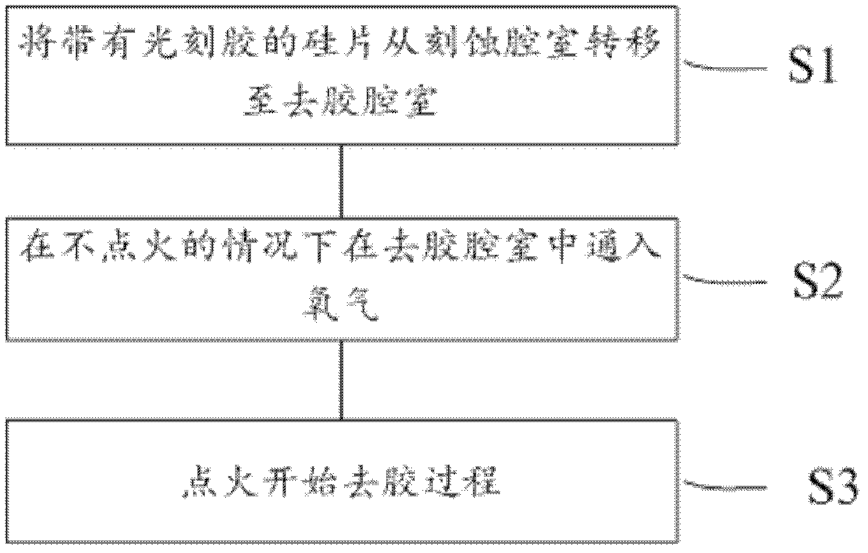
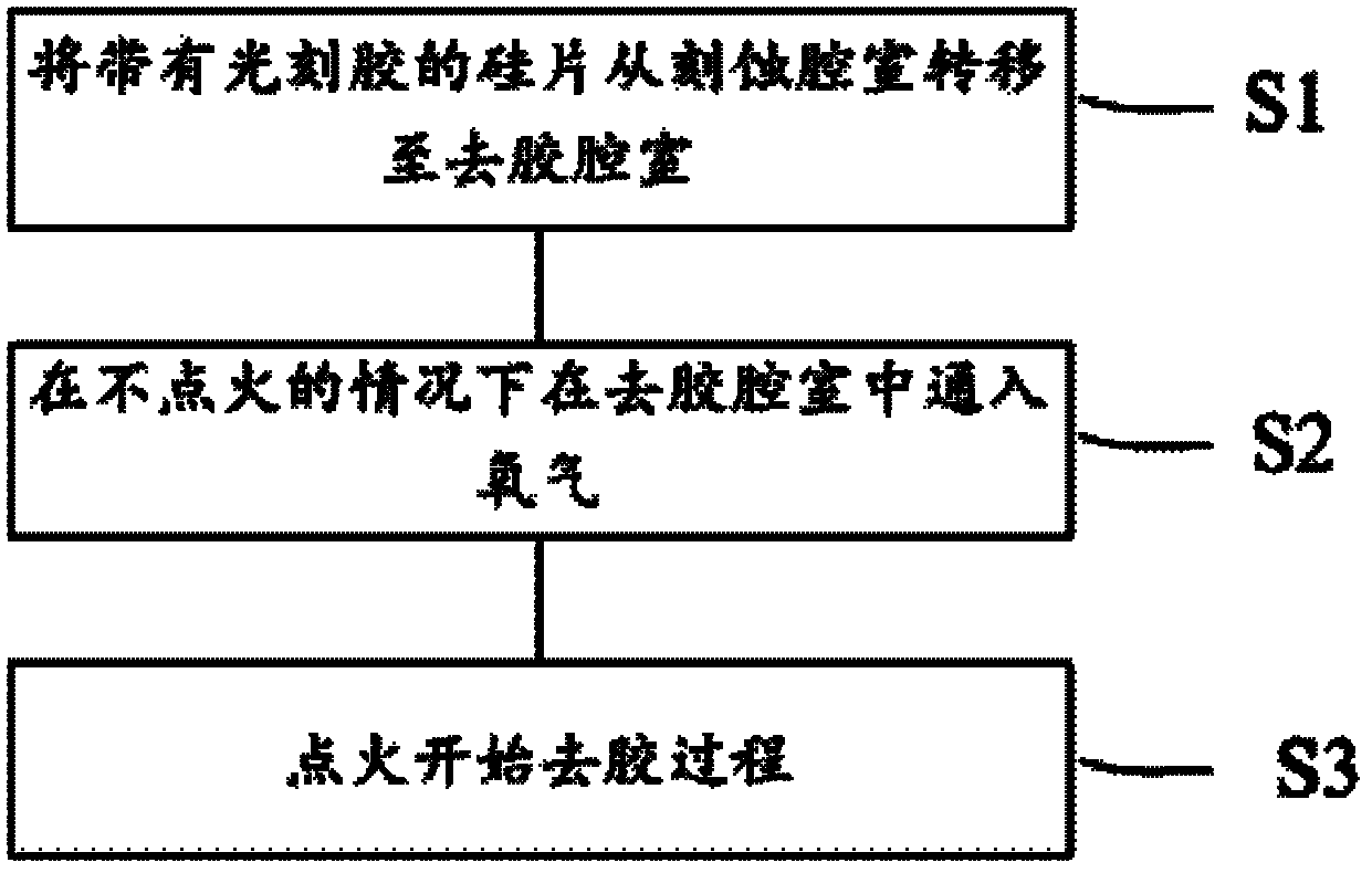
[0018] In order to make the content of the present invention clearer and easier to understand, the content of the present invention will be described in detail below in conjunction with specific embodiments and accompanying drawings.

[0019] The inventors of the present invention have found that in the prior art photoresist removal method, the reason for the formation of photoresist residue is due to the temperature of the silicon wafer below the photoresist when the photoresist is removed in the stripping chamber chamber. The burning rate of the photoresist is not high enough so that part of the photoresist has cured to form a photoresist residue such as photoresist polymer before the photoresist is completely burned out.

[0020] More specifically, the temperature of the stripping chamber is generally 250°C or more higher than the melting point of the photoresist; therefore, when the wafer is transferred from the etch chamber to the stripping chamber, the wafer and stripping...


PUM


Abstract

The invention provides a photoresist removing method, a metal wire etching method and a production method of an integrated circuit. The photoresist removing method provided by the invention comprises the following steps: transferring a silicon wafer with photoresist to a photoresist removing chamber from an etching chamber; introducing oxygen into the photoresist removing chamber in the case of not igniting; and then, igniting and starting the photoresist removing process. According to the photoresist removing method provided by the invention, oxygen is introduced before igniting, so that temperatures of the silicon wafer and the photoresist are both raised to a certain temperature to reach an enough etching speed and oxygen serving as a combustion-supporting gas fully contacts the photoresist serving as a comburant; therefore, in the photoresist removing process after igniting, since the temperature of the silicon wafer is raised and the oxygen is fully mixed with the photoresist, the photoresist is combusted completely and the generation of photoresist residues can be avoided effectively.

Description

technical field [0001] The present invention relates to the field of semiconductor manufacturing, and more specifically, the present invention relates to a photoresist removal method, a metal line etching method using the photoresist removal method, and a photoresist removal method or the metal line etching method using the photoresist removal method. Integrated circuit fabrication method by wire etching method. Background technique [0002] During the fabrication of semiconductor integrated circuits (ICs), metal wiring is deposited to connect individual integrated circuit components, and to connect the integrated circuits to pads. These metal wirings are formed by physical deposition of metal materials (eg, Al, AlCu, Ti / TiN, etc.). [0003] During the formation of the metal wiring, a photoresist (also referred to as photoresist) is applied to define the pattern of the metal wiring, that is, the metal wiring is etched according to the defined pattern of the photoresist. Fo...

Claims


Application Information

Patent Timeline
Patent Type & Authority Applications(China)
IPC IPC(8): H01L21/311H01L21/3213
Inventor 彭精卫王敬平
Owner SHANGHAI HUAHONG GRACE SEMICON MFG CORP
Why Eureka
Try Eureka