
Forming a contact in a thin-film device

a thin-film device and contact technology, applied in the manufacture/treatment of galvano-magnetic devices, semiconductor devices, electrical apparatus, etc., can solve the problems of flash memory problems, high density and greater capacity of non-volatile memories, and the writing speed remains on the order of microseconds

Inactive Publication Date: 2005-08-04
DATA QUILL
View PDF8 Cites 16 Cited by
  • Summary
  • Abstract
  • Description
  • Claims
  • Application Information

AI Technical Summary

Problems solved by technology

In particular, realization of higher density and greater capacity of non-volatile memories has become a more important issue for the art of replacing such a hard disk or an optical disk which is difficult to be down-sized due to presence of moving elements.
Nevertheless, flash memory is problematic in the sense that the writing speed remains on the order of micro-seconds and the re-write cycles are limited.
FRAM is problematic in the sense that it is difficult to scale to ultra-high density and the re-writable cycles are insufficient.
Conventional MRAM manufacturing methods typically do not utilize a lift-off technique.

Method used


Image

  • Forming a contact in a thin-film device
  • Forming a contact in a thin-film device
  • Forming a contact in a thin-film device

Examples


Embodiment Construction

[0026] The present invention relates to a method and system for forming a contact in a thin-film device. The following description is presented to enable one of ordinary skill in the art to make and use the invention and is provided in the context of a patent application and its requirements. Various modifications to the embodiments and the generic principles and features described herein will be readily apparent to those skilled in the art. Thus, the present invention is not intended to be limited to the embodiment shown but is to be accorded the widest scope consistent with the principles and features described herein.

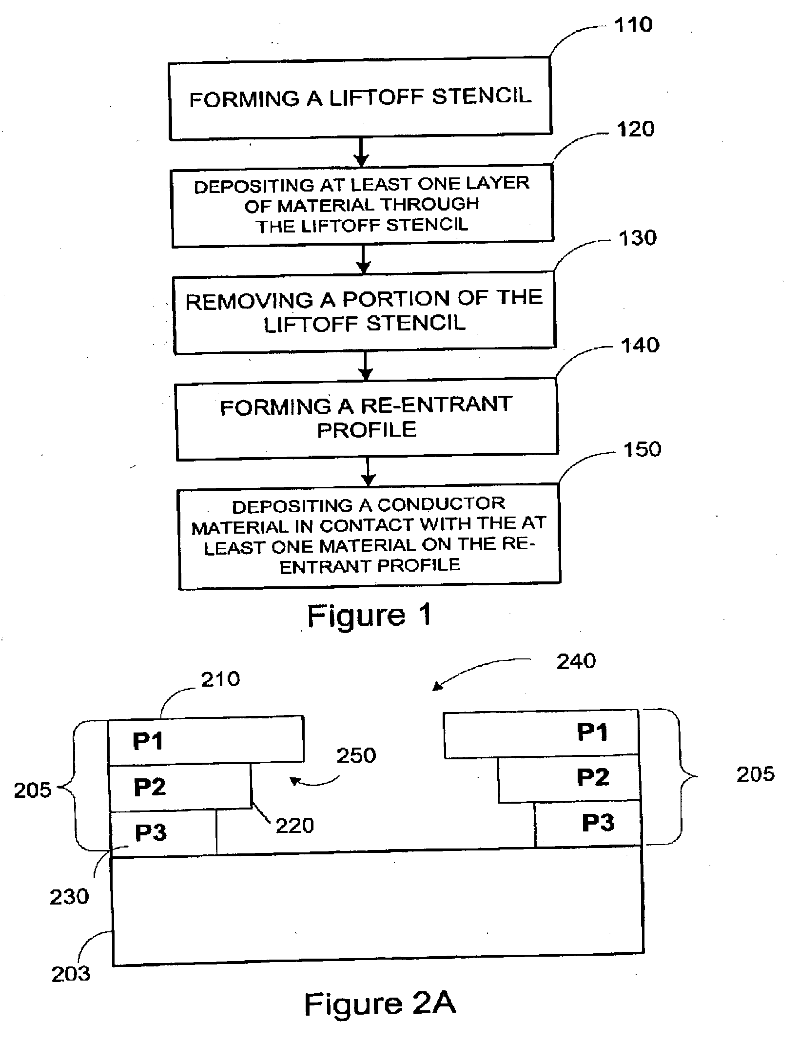
[0027] As shown in the drawings for purposes of illustration, a method and system for forming a contact in a thin-film device is disclosed. In accordance with an embodiment, a re-entrant profile is implemented in conjunction with the utilization of a lift-off stencil. By implementing a re-entrant profile in conjunction with the utilization of a lift-off stencil, mat...


PUM


Abstract

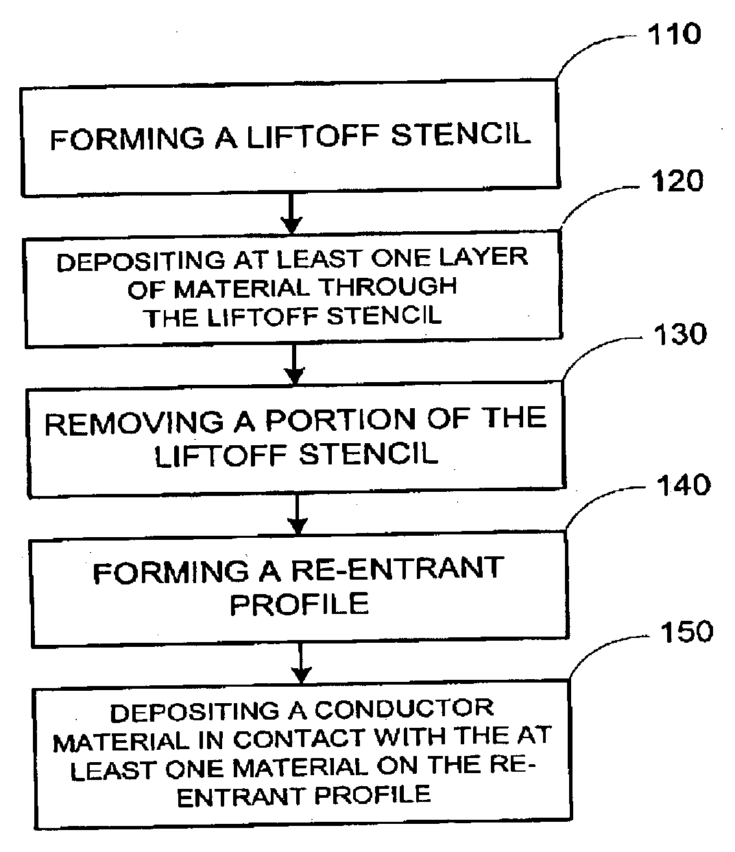
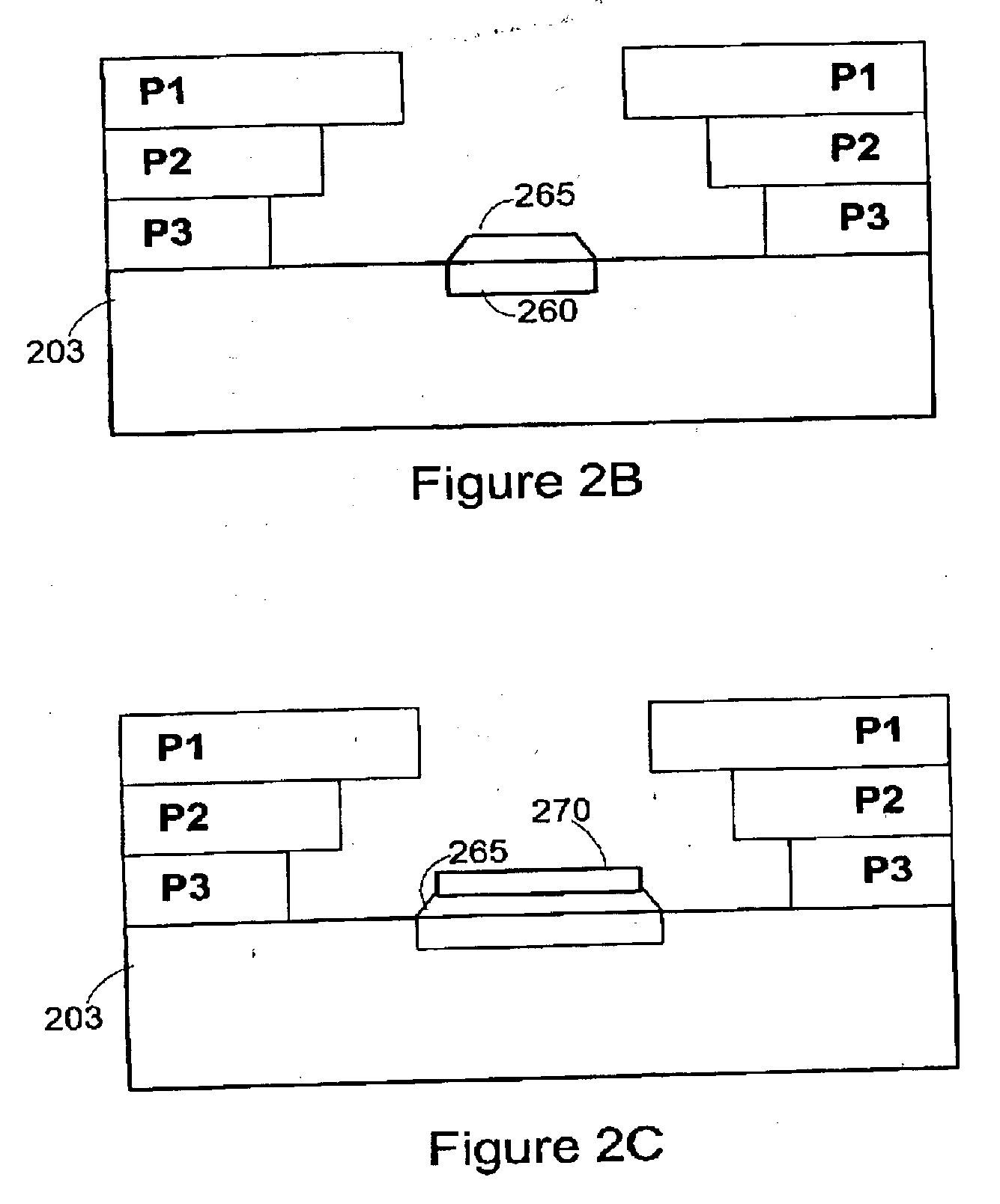
An aspect of the present invention is a method of forming a contact in a thin-film device. The method includes forming a liftoff stencil, depositing at least one material through the liftoff stencil, removing a portion of the liftoff stencil, forming a re-entrant profile with the remaining portion of the liftoff stencil and depositing a conductor material in contact with the at least one material on the re-entrant profile.

Description

FIELD OF THE INVENTION [0001] The present invention relates generally to thin-film devices and more particularly to a method and system for forming a contact in a thin-film device. BACKGROUND OF THE INVENTION [0002] Rapid growth of information communicating apparatuses, such as a PDA (Personal Digital Assistant), demands higher integration, faster speed, and lower power consumption for memory elements and logic elements available for constituting these communicating apparatuses. In particular, realization of higher density and greater capacity of non-volatile memories has become a more important issue for the art of replacing such a hard disk or an optical disk which is difficult to be down-sized due to presence of moving elements. [0003] Current non-volatile memories include flash memory, which is based on semiconductor technology and FRAM (Ferro-electric Random Access Memory), which is based on a ferro-dielectric technology. Nevertheless, flash memory is problematic in the sense t...

Claims


Application Information

Patent Timeline
IPC IPC(8): H01L21/027H01L21/033H01L21/311H01L21/44H01L43/12
CPCH01L21/0272H01L21/0331Y10S438/951H01L43/12H01L21/31144H10N50/01
Inventor SHARMA, MANISHANTHONY, THOMAS C.LEE, HEON
Owner DATA QUILL
Learn More