Plasma chemical vapor deposition system and method for coating both sides of substrate

Inactive Publication Date: 2005-08-04
SAMSUNG ELECTRONICS CO LTD
View PDF11 Cites 47 Cited by
  • Summary
  • Abstract
  • Description
  • Claims
  • Application Information

AI Technical Summary

Benefits of technology

[0028] According to another aspect of the present invention, there is provided a plasma chemical vapor deposition method comprising disposing a substrate on a substrate holder in a central area of a chamber provided with a gas injection hole and a gas ex

Problems solved by technology

However, the high stress may be fatal for the plastic substrate, deteriorating the alignment and cracking the deposited layers.
Therefore, when the silicon oxide layer is coated on a first side of the substrate, the substrate is to be severely flexed.
As a result, even when the substrate is turned over and the silicon oxide layer is coated on a second side of the substrate, it is often cracked at the flexed portion.
However, such a capacitive plasma CVD system has a problem in that a back plate functioning as the anode should be disp

Method used


Image

  • Plasma chemical vapor deposition system and method for coating both sides of substrate
  • Plasma chemical vapor deposition system and method for coating both sides of substrate
  • Plasma chemical vapor deposition system and method for coating both sides of substrate

Examples


Embodiment Construction

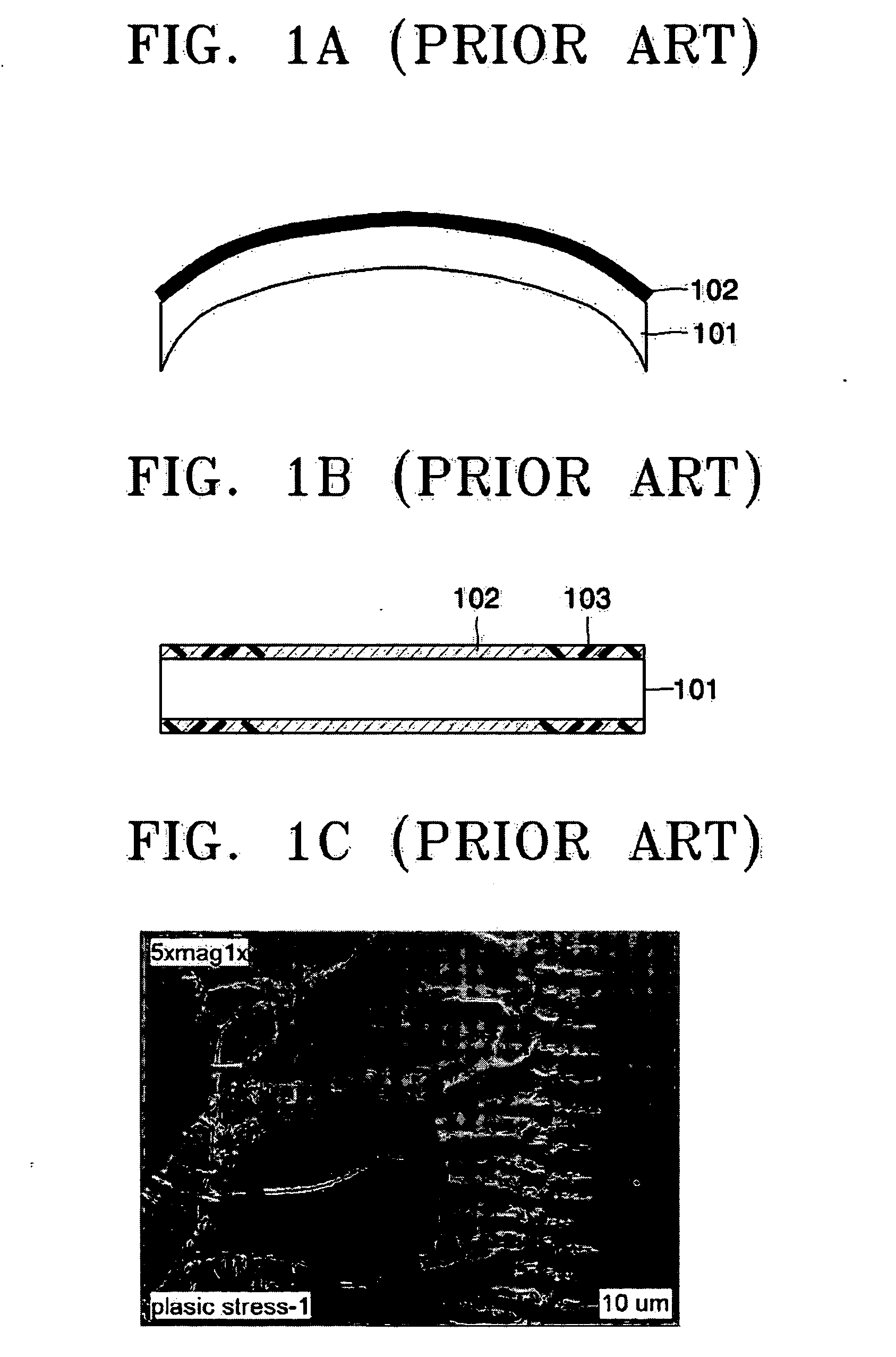
[0040] The present invention will now be described more fully with reference to the accompanying drawings, in which exemplary embodiments of the invention are shown. The invention may, however, be embodied in many different forms and should not be construed as being limited to the embodiments set forth herein; rather, these embodiments are provided so that this disclosure will be thorough and complete, and will fully convey the concept of the invention to those skilled in the art.

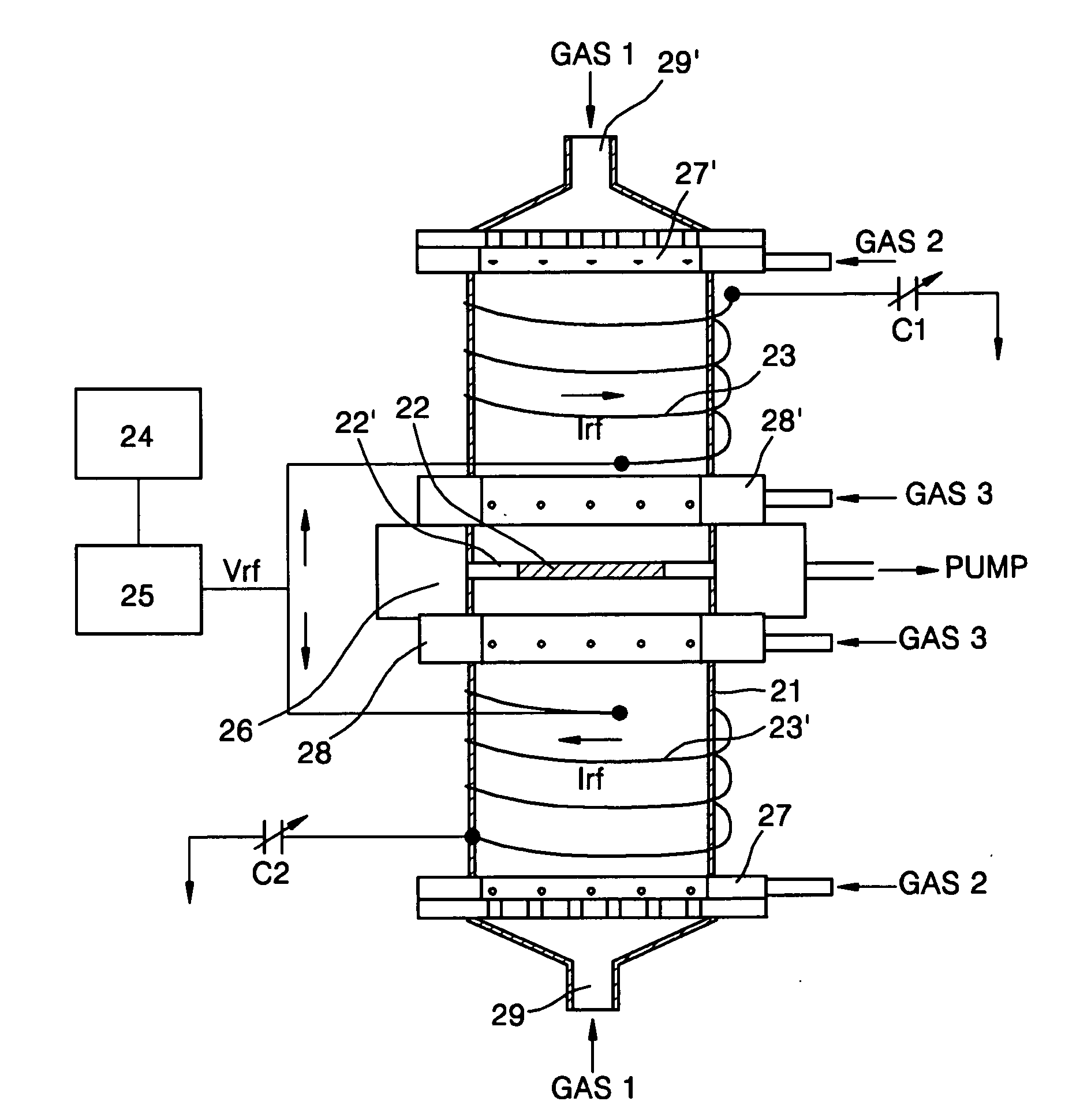
[0041] Referring first to FIG. 2A, a substrate 22 to be deposited with a desired material is mounted on a substrate holder 22′ in a chamber 21. First and second coils 23 and 23′generating an induced magnetic field are disposed around upper and lower circumferences of the chamber 21 with reference to the substrate 22. The first and second coils 23 and 23′ may be helical type coils or flat antenna type coils facing each other. First ends of the coils 23 and 23′ are electrically connected to a matching box 25...


PUM

PropertyMeasurementUnit
Magnetic fieldaaaaaaaaaa
Sizeaaaaaaaaaa
Distanceaaaaaaaaaa

Abstract

A plasma chemical vapor deposition system includes a chamber provided with gas injection holes, a gas exhaust unit mounted on the chamber, a substrate holder disposed on a central area of the chamber to support a substrate in a state where both sides of the substrate are exposed, and first and second coils generating induced magnetic fields. The first and second coils are disposed around upper and lower outer circumferences of the chamber, respectively.

Description

BACKGROUND OF THE INVENTION [0001] Priority is claimed to Korean Patent Application No. 10-2004-0006105, filed on Jan. 30, 2004, in the Korean Intellectual Property Office, the disclosure of which is incorporated herein in its entirety by reference. [0002] 1. Field of the Invention [0003] The present invention relates to plasma chemical vapor deposition (CVD) system and method for coating both sides of a substrate, and more particularly, to plasma CVD system and method that can uniformly coat both sides of a substrate with material. [0004] 2. Description of the Related Art [0005] Generally, a plastic substrate is lighter than a glass substrate, and is not being easily broken. Therefore, in recent years, plastic substrates have been actively developed as a substitution of the glass substrate used for a thin film transistor (TFT) liquid crystal display (LCD) as well as a material for an organic electroluminiscent (EL) substrate. Since the plastic substrate has less rigidity compared w...

Claims


Application Information

Patent Timeline
IPC IPC(8): H01L21/205C23C16/44C23C16/455C23C16/507H01L21/31H01L21/316
CPCC23C16/4412C23C16/455H01L21/31612C23C16/507C23C16/45502H01L21/02164A47K10/421B65D83/0805
Inventor PARK, YOUNG-SOOTOLMACHEV, YURI
Owner SAMSUNG ELECTRONICS CO LTD
Why Eureka
Try Eureka