

Plasma display module
- Summary
- Abstract
- Description
- Claims
- Application Information
AI Technical Summary
Benefits of technology
Problems solved by technology
Method used
Image

Examples
first embodiment
[0043] Turning now to FIGS. 3 and 4, FIG. 3 is an exploded perspective view illustrating a plasma display module according to the present invention and FIG. 4 is a cross-sectional view illustrating the plasma display module of FIG. 3., For convenience of explanation, in FIG. 3, wires and driving devices mounted on the plasma display module are omitted.
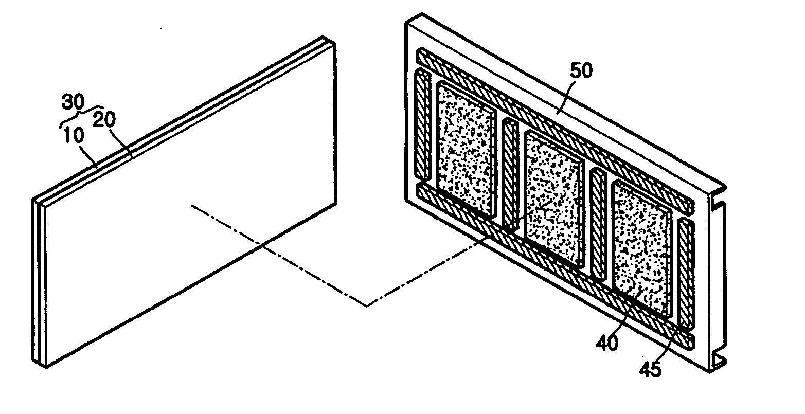
[0044] Referring to FIG. 4, a plasma display module includes a PDP 130 on which an image is displayed, a chassis base 150, and a heat dissipating sheet 140 located between the PDP 130 and the chassis base 150. The PDP 130 is an image display unit on which images are displayed by the use of a discharge effect. The PDP 130 includes a first panel 110 and a second panel 120.
[0045] Since the PDP 130 generates heat during operation, the heat dissipation of the PDP 130 is accelerated by mounting the chassis base 150 on a rear surface of the PDP 130. For this purpose, the chassis base 150 can be formed of a material having a high thermal cond...
second embodiment
[0054] Turning now to FIGS. 7 and 8, FIG. 7 is an exploded perspective view illustrating a plasma display module according to the present invention and FIG. 8 is a cross-sectional view illustrating the plasma display module of FIG. 7. Referring to FIG. 7, an attach / detachment structure 280 includes a first combining unit 280a and a second combining unit 280b. Here, the first combining unit 280a and the second combining unit 280b are attached by a hinge structure. Hook holes 280b′ perforate the second combining unit 280b, and guide pins 251 are formed on an upper part of a bending unit 250a. The attach / detachment structure 280 is hooked to the chassis base 250 by inserting the guide pins 251 through the hook holes 280b′ by rotating the second combining unit 280b.
[0055] Referring to FIG. 8, the first combining unit 280a, which is located between the PDP 230 and the chassis base 250, is attached to a rear surface of the PDP 230 by an adhesive element 270. In this manner, since the sec...
fourth embodiment
[0059] Turning now to FIG. 14, FIG. 14 is a cross-sectional view illustrating a first modified version of the plasma display module of the present invention. Referring to FIG. 14, the first combining unit 480a and the second combining unit 480b can be attached by a hinge. At this time, the first and second combining units 480a and 480b can be formed perpendicular to each other regardless of the material of the attach / detachment structure 480. Also, the wires 462 located between the second combining unit 480b and the chassis base 450 can be protected from impact by rounding an outer edge 480ba of the second combining unit 480b.
[0060]FIG. 15 is a cross-sectional view illustrating a second modified version of the plasma display module of the fourth embodiment of the present invention. Referring to FIG. 15, the attach / detachment structure 480 includes the frame unit 480c that covers an edge of the PDP 430 and the first and second combining units 480a and 480b that are bent at the frame...
PUM
 Abstract
Description
Claims
Application Information