Wiring substrate produced by transfer material method

a technology of transfer material and wiring substrate, which is applied in the direction of transportation and packaging, printed element electric connection formation, and semiconductor/solid-state device details, etc., can solve the problems of high-density mounting limitation, difficult to incorporate passive components into the substrate, and breakage of the line between the wiring pattern and the connection portion, so as to achieve radical freedom in the design of the electric circuit

Inactive Publication Date: 2005-08-25
PANASONIC CORP
View PDF30 Cites 54 Cited by
  • Summary
  • Abstract
  • Description
  • Claims
  • Application Information

AI Technical Summary

Benefits of technology

[0027] It is an object of the present invention to provide a wiring pattern formation and transfer material, which transfers a fine wiring pattern to a substrate, more particularly, to a wiring pattern formation and transfer material capable of transferring a fine wiring pattern to a substrate easily and reliably and at a low cost. In addition, in order to advance the high density mounting, it is important not only to make a wiring pattern to be fine but also to form and mount circuit components connecting to a wiring pattern. Conventionally, a passive component such as an inductor, a capacitor, a resistor, or the like, is mounted generally on the surface of the substrate. And it was difficult to incorporate such passive components into the substrate. Therefore, there was a limitation to high density mounting.
[0029] It is another object of the present invention to provide a wiring pattern formation and transfer material for incorporating a fine wiring pattern or circuit components into a circuit substrate, more specifically, a wiring pattern formation and transfer material capable of mounting a circuit component etc. on the circuit substrate accurately and at a low cost.
[0033] Furthermore, in order to achieve the object, a first method for producing a transfer material of the present invention includes forming a peel layer on a first metal layer, forming a second metal layer on the peel layer, and etching the second metal layer, the peel layer and the surface portion of the first metal layer by a chemical etching process, thereby forming the second metal layer and the peel layer into the wiring pattern, and at the same time, forming a convex and concave portion having a convex portion corresponding to the wiring pattern on the surface portion of the first metal layer. With the transfer material of the second configuration, it is possible to form circuit components such as an inductor, a capacitor, and a resistor, etc. by printing in one process. In particular, the formation of the resistor becomes easy. Moreover, the circuit components are not necessarily limited to these passive materials, and an active component such as a semiconductor chip, etc. can be formed.
[0034] Furthermore, mounting of the circuit components by using a solder etc. becomes unnecessary, thus simplifying a mounting process. Furthermore, since the soldering connection is reduced, the reliability of the wiring substrate can be improved. Furthermore, since the circuit components are formed on the transfer material by printing, as compared with the case where component chips are mounted by soldering, the height of the circuit components can be reduced, thus facilitating the transfer while embedding the components into the substrate and the integration of the components into the substrate. Furthermore, the circuit components can be placed freely, for example, it is possible to make the wiring distance from the circuit components to the integrating capacitor, etc. the shortest, thereby improving the high frequency property.
[0035] Furthermore, in the transfer material of the second configuration, after transfer, by forming new second metal layer or wiring pattern or component pattern on the first metal layer that is a peeled carrier, it is possible to reuse the first metal layer. And the configuration of the wiring pattern is not particularly limited. Therefore, low cost can be realized, and furthermore, it is useful from the viewpoint of industrial applicability.
[0047] With the transfer material of the second configuration, it is possible to transfer the circuit components onto any of the layers of the multi-layered substrate, and further the components can be placed freely. Therefore, the degree of freedom in designing the electric circuit is radically improved.

Problems solved by technology

And it was difficult to incorporate such passive components into the substrate.
Therefore, there was a limitation to high density mounting.
However, in embedding the passive components, etc. into the substrate, there arise some problems of breakage of line between the wiring pattern and the connection portion, the dislocation of chip, and the like.

Method used


Image

  • Wiring substrate produced by transfer material method
  • Wiring substrate produced by transfer material method
  • Wiring substrate produced by transfer material method

Examples


first embodiment

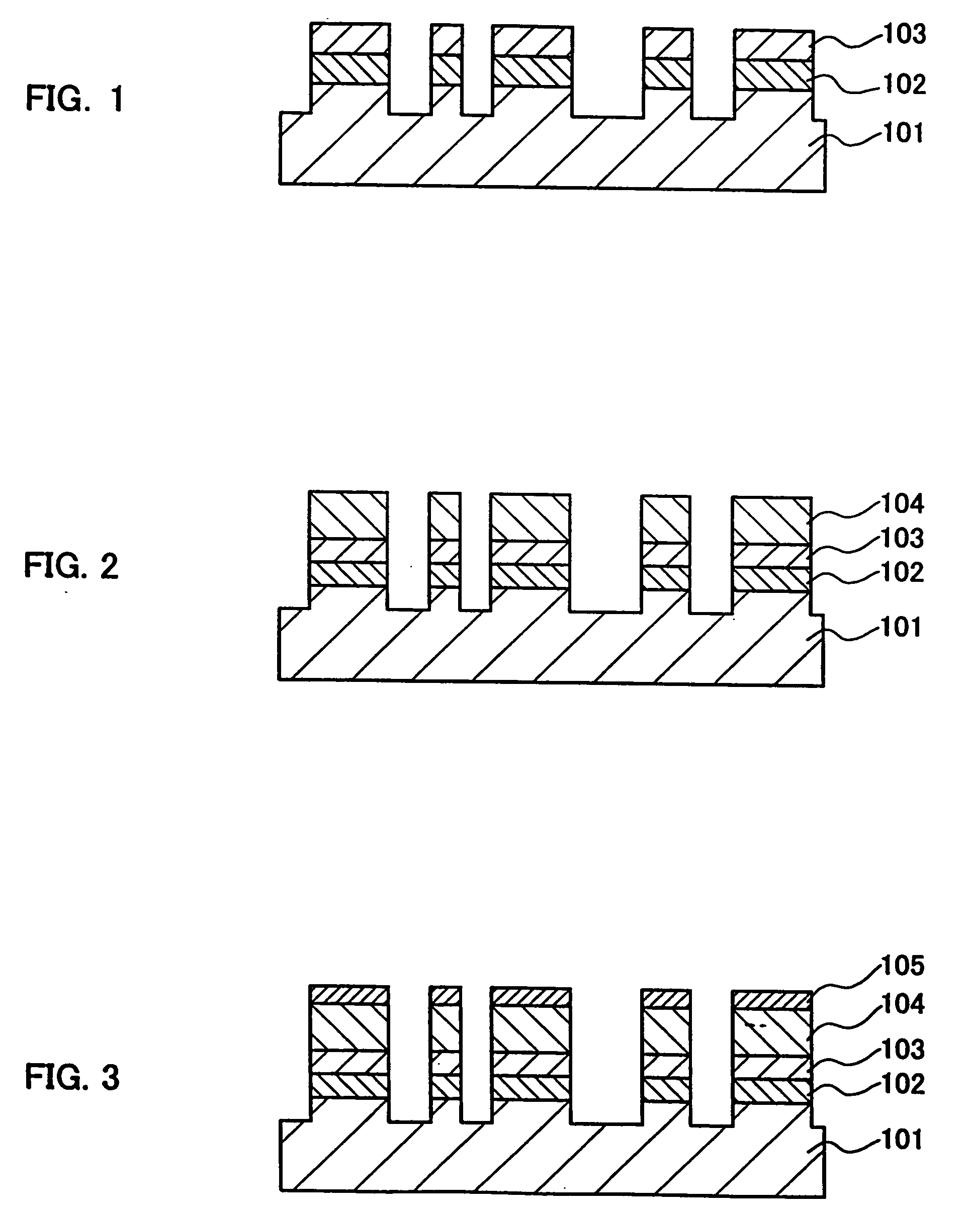
[0075] One example of a wiring pattern formation and transfer material according to a first embodiment of the present invention (hereinafter, a first transfer material will be referred to) is described. FIG. 1 is a cross-sectional view showing a schematic configuration of the first transfer material.

[0076] As shown in FIG. 1, the first transfer material includes a first metal layer 101 having a concave and convex portion (for example, the height of the convex portion is about 1 to 12 μm) on a surface portion thereof. The convex portion of the first metal layer 101 corresponds to a wiring pattern. A peel layer 102 made of an organic layer or a metal plating layer and a second metal layer 103 are formed on the convex portions. Namely, the first transfer material has a three-layered structure in which the first metal layer 101 is adhered to the second metal layer 103 with the peel layer 102 sandwiched therebetween.

[0077] In the first transfer material, the second metal layer 103 is a...

second embodiment

[0084] One example of a transfer material according to a second embodiment of the present invention (hereinafter, a second transfer material will be referred to) is described. FIG. 2 is a cross-sectional view showing a schematic configuration of the second transfer material.

[0085] As shown in FIG. 2, the second transfer material includes a first metal layer 101 having a concave and convex portion on a surface portion thereof. The convex portion corresponds to a wiring pattern. The second transfer material has a four-layered structure in which a peel layer 102 made of an organic layer or a metal plating layer and a second metal layer 103 are formed on the convex portion, and further a third metal layer 104 is formed on the second metal layer 103. The first metal layer 101 is adhered to the second metal layer 103 with the peel layer 102 sandwiched therebetween.

[0086] In the second transfer material, the second metal layer 103 and the third metal layer 104 make a two-layered wiring p...

third embodiment

[0103] One example of a transfer material according to a third embodiment of the present invention (hereinafter, a third transfer material will be referred to) is described. FIG. 3 is a cross-sectional view showing a schematic configuration of the third transfer material.

[0104] As shown in FIG. 3, the third transfer material includes a first metal layer 101 having a concave and convex portion on a surface portion thereof. The convex portion corresponds to a wiring pattern. The third transfer material has a five-layered structure in which a peel layer 102 made of an organic layer or a metal plating layer and a second metal layer 103 are formed on the convex portion, further a third metal layer 104 is formed thereon, and further a fourth metal layer 105 is formed thereon. The first metal layer 101 is adhered to the second metal layer 103 via the peel layer 102.

[0105] In the third transfer material, the second metal layer 103, the third metal layer 104 and the fourth metal layer 105 ...


PUM


Abstract

A transfer material capable of transferring a fine wiring pattern to a substrate reliably and easily. The transfer material includes at least three layers of a first metal layer as a carrier, a second metal layer that is transferred to the substrate as a wiring pattern, and a peel layer adhering the first and second metal layers releasably. On the surface portion of the first metal layer, a concave and convex portion corresponding to the wiring pattern is formed, and the peel layer and the second metal layer are formed on a region of the convex portions.

Description

BACKGROUND OF THE INVENTION [0001] 1. Field of the Invention [0002] The present invention relates to a transfer material for transferring a fine wiring pattern or circuit components to a substrate, and a method for producing the same. Furthermore, the present invention relates to a wiring substrate on which a wiring pattern or a circuit component is formed and a method for producing the same. [0003] 2. Related Background Art [0004] Recently, with a demand for high performance and miniaturization of electronic equipment, high-density and high-performance semiconductor devices increasingly have been desired. This leads to a demand for a small size and high density circuit substrate on which such semiconductor devices are to be mounted. [0005] In order to meet such demands, a connection method using inner via holes (IVHs) that can connect between wiring patterns of large-scale integrated circuits (LSIs) or circuit components in the shortest distance has been developed in various fields...

Claims


Application Information

Patent Timeline
Patent Type & Authority Applications(United States)
IPC IPC(8): H05K1/03H05K1/16H05K3/20H05K3/40
CPCH01L2221/68345Y10T29/49179H01L2221/68363H01L2924/0102H01L2924/01078H05K1/0306H05K1/16H05K1/162H05K1/165H05K1/167H05K3/20H05K3/205H05K3/4061H05K3/4069H05K2203/1461H01L2924/0002H01L2221/68359Y10T29/49149Y10T29/49208Y10T29/49213Y10T428/12486H01L2924/00
Inventor SUGAYA, YASUHIROKOMATSU, SHINGOHIRANO, KOICHINAKATANI, SEIICHIMATSUOKA, YASUYUKIASAHI, TOSHIYUKIYAMASHITA, YOSHIHISA
Owner PANASONIC CORP
Why Eureka
Try Eureka