Semiconductor light emitting device and method for manufacturing same

a technology of light-emitting devices and semiconductors, which is applied in the direction of semiconductor devices, thermoelectric device junction materials, electrical equipment, etc., can solve the problems of color tone variation, more visible color tone variation, and different thicknesses, and achieve uniform color tone

Inactive Publication Date: 2005-09-01
KK TOSHIBA
View PDF10 Cites 18 Cited by
  • Summary
  • Abstract
  • Description
  • Claims
  • Application Information

AI Technical Summary

Benefits of technology

[0008] The present invention is based on recognition of that problem. It is therefore an object of the invention to provide a semiconductor light emitting device comprising at least a semiconductor light emitting element and a fluorescent material portion including a fluorescent material excited by light from the semiconductor light emitting element and ensuring a uniform color tone.

Problems solved by technology

These devices, however, are subjected to differences in thickness of fluorescent materials through which light from semiconductor light emitting elements pass, and involve the problem of variance in color tone depending on view angles.
Especially with white light emitting devices, variance in color tone is more visible, and it has been inconvenient that color tone changes depending upon view angles.

Method used


Image

  • Semiconductor light emitting device and method for manufacturing same
  • Semiconductor light emitting device and method for manufacturing same
  • Semiconductor light emitting device and method for manufacturing same

Examples


first embodiment

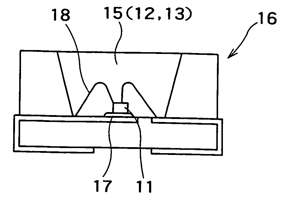
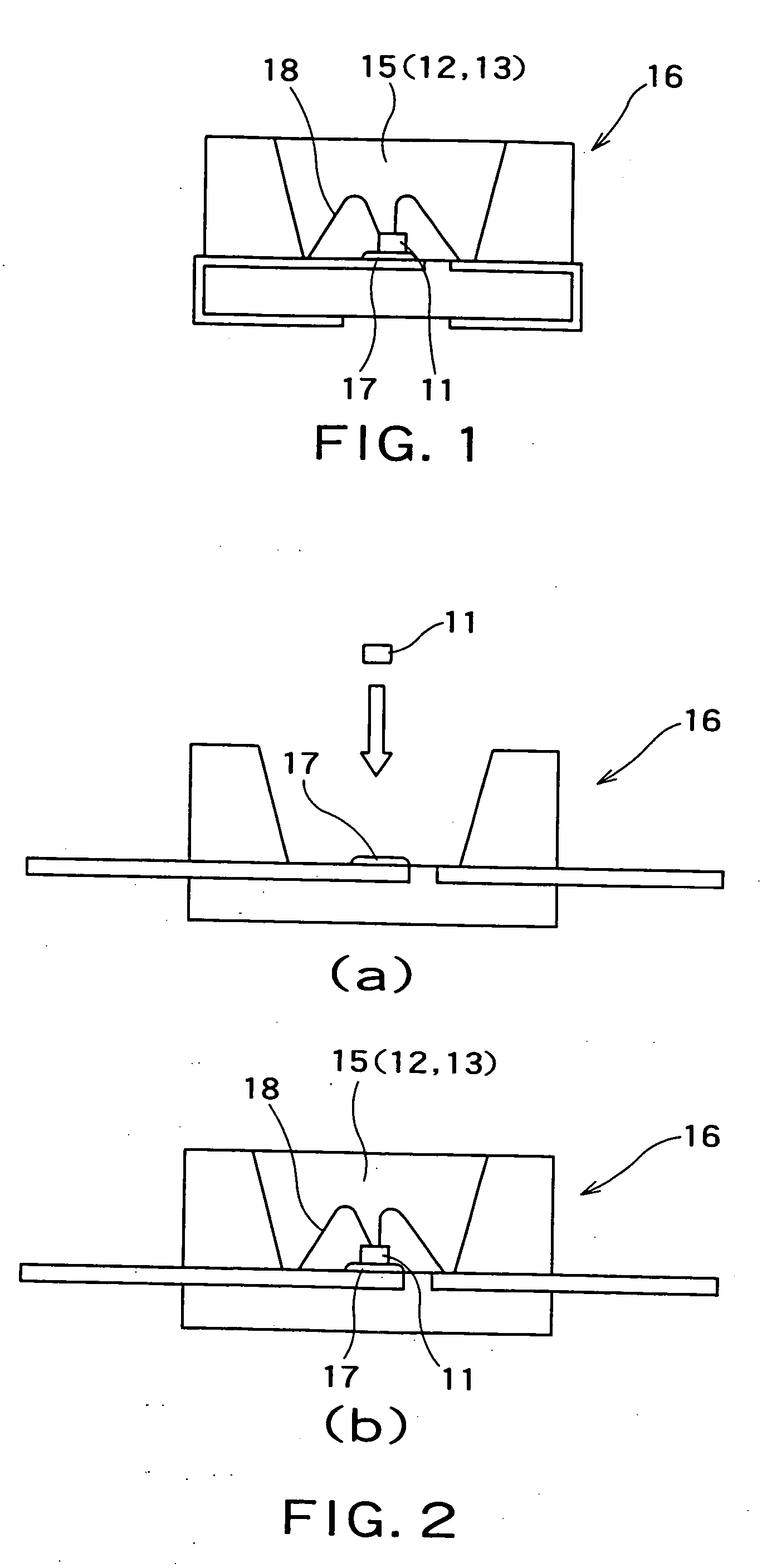
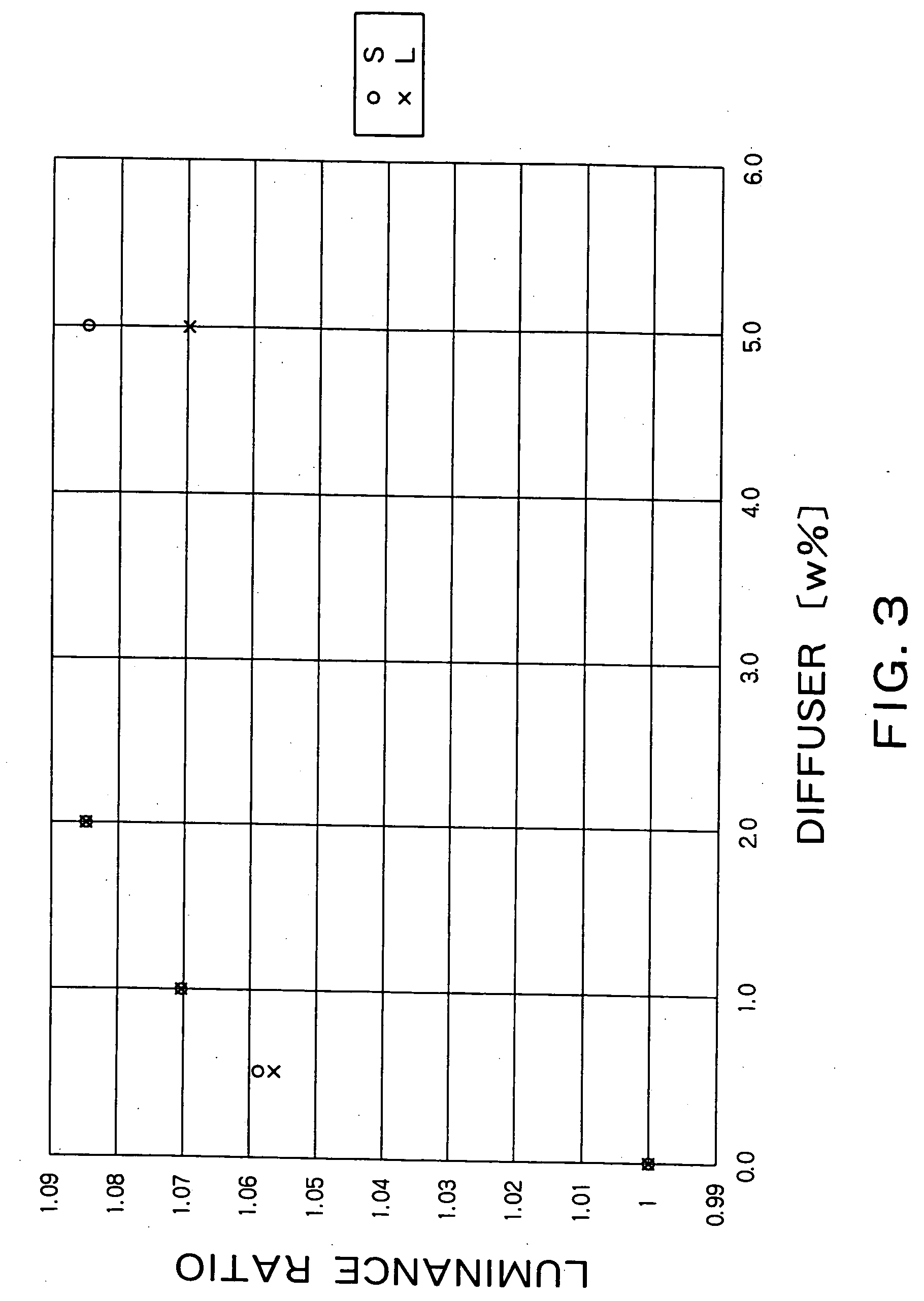
[0055] The semiconductor light emitting device taken as the first embodiment is a semiconductor light emitting device for emitting white light, which is called a surface mounted device (hereinafter abbreviated as SMD). One of features of the semiconductor light emitting device according to the instant embodiment lies in, as shown in FIG. 1, introducing an appropriate amount of diffuser 13 into silicone resin used as sealing resin 15. Used as a semiconductor light emitting element 11 is an element made of GaN materials and emitting ultraviolet light when a current is injected. Used as fluorescent materials 12 are three kinds of fluorescent materials, namely, a red fluorescent material excited by ultraviolet emission to emit red light, a green fluorescent material excited by ultraviolet emission to emit green light, and a blue fluorescent material excited by ultraviolet emission to emit blue light (hereinafter abbreviated as RGB fluorescent materials). Used as the diffuser 13 is alumi...

second embodiment

[0078] A semiconductor light emitting device according to the second embodiment comprises, as shown in FIG. 5, a sealing resin 25, a binder 24 in which fluorescent materials 22 and a diffuser 23 are mixed, which are formed as separate elements. Configuration of the product, kind of the semiconductor light emitting element 21, kinds of the fluorescent materials 22 and kind of the diffuser 23 are the same as those of the first embodiment.

[0079]FIG. 5 is a schematic cross-sectional view of the semiconductor light emitting device according to the second embodiment. The semiconductor light emitting element 21 made of GaN materials and emitting ultraviolet light upon injection of a current is bonded inside a reflector of a frame 26 with an adhesive 27 such as silver paste. Both p and n electrodes of the semiconductor light emitting device 21 are connected to the frame 26 by a wire 28 of Au, for example. A lower portion inside the reflector of the frame 26 in the view of FIG. 5 is filled ...

third embodiment

[0097] A semiconductor light emitting device according to the third embodiment comprises, as shown in FIG. 8, a binder 34 in which fluorescent materials 32, an adherent or cohesive medium 33a in which a diffuser 33 is mixed, and sealing resin 35, which are formed as separate elements. Configuration of the product, kind of the semiconductor light emitting element 31, kinds of the fluorescent materials 32 and kind of the diffuser 33 are the same as those of the second embodiment.

[0098]FIG. 8 is a schematic cross-sectional view of the semiconductor light emitting device according to the third embodiment. The semiconductor light emitting element 31 made of GaN materials and emitting ultraviolet light upon injection of a current is bonded inside a reflector of a frame 36 with an adhesive 37 such as silver paste. Both p and n electrodes of the semiconductor light emitting device 31 are connected to the frame 36 by a wire 38 of Au, for example. A lower portion inside the reflector of the ...


PUM


Abstract

A semiconductor light emitting device ensuring a uniform color tone comprises a semiconductor light emitting element that emits light of a first wavelength upon injection of a current, a fluorescent material portion that contains a fluorescent material excited by light of the first wavelength to emit light of a second wavelength, and a diffuser mixed in an appropriate material around the semiconductor light emitting element.

Description

CROSS REFERENCE TO RELATED APPLICATION [0001] This application is based upon and claims the benefit of priority from the prior Japanese Patent Application No. 2000-232050, filed on Jul. 31, 2000, the entire contents of which are incorporated herein by reference. BACKGROUND OF THE INVENTION [0002] 1. Field of the Invention [0003] This invention relates to a semiconductor light emitting device and its manufacturing method, and more particularly, to a semiconductor device using a fluorescent material and its manufacturing method. [0004] 2. Related Background Art [0005] Light emitting devices combining a semiconductor light emitting element like LED (light emitting diode) and a fluorescent material are remarked as inexpensive and long-life light emitting devices, and they are being used widely. Among semiconductor light emitting devices, those for emitting white light are especially regarded hopeful for various ways of use as light emitting devices that can substitute for fluorescent la...

Claims


Application Information

Patent Timeline
Patent Type & Authority Applications(United States)
IPC IPC(8): H01L33/32H01L33/34H01L33/44H01L33/50H01L33/54H01L33/56H01L33/62
CPCH01L33/501H01L2224/45144H01L33/56H01L2933/0091H01L2224/8592H01L2224/92247H01L33/54H01L2224/83192H01L24/97H01L2224/32245H01L2224/48091H01L2224/48247H01L2224/48257H01L2224/73265H01L2924/00014H01L2924/00H01L2924/12041H01L24/73H01L2224/97H01L2924/181H01L2924/00012
Inventor FURUKAWA, CHISATOMORISHITA, MASAYUKI
Owner KK TOSHIBA
Why Eureka
Try Eureka