Method for selectively stressing MOSFETs to improve charge carrier mobility

a selective stressing and charge carrier technology, applied in the field of mosfet device formation, can solve the problems of limited success of approaches, increased limitation, and thickness of dielectric stress layer, and achieve the effect of improving charge mobility and method

Inactive Publication Date: 2005-09-15
TAIWAN SEMICON MFG CO LTD
View PDF2 Cites 83 Cited by
  • Summary
  • Abstract
  • Description
  • Claims
  • Application Information

AI Technical Summary

Benefits of technology

[0008] To achieve the foregoing and other objects, and in accordance with the purposes of the present invention, as embodied and broadly des

Problems solved by technology

In addition, ion implatation and annealing processes following formation of the gate structure typically introduce additional stresses into the polysilicon gate structure which are translated into the underlying channel region altering device performance.
These approaches have met with limited success, however, since the formation of the stressed dielectric layer typically has a degrading electric

Method used


Image

  • Method for selectively stressing MOSFETs to improve charge carrier mobility
  • Method for selectively stressing MOSFETs to improve charge carrier mobility
  • Method for selectively stressing MOSFETs to improve charge carrier mobility

Examples


Embodiment Construction

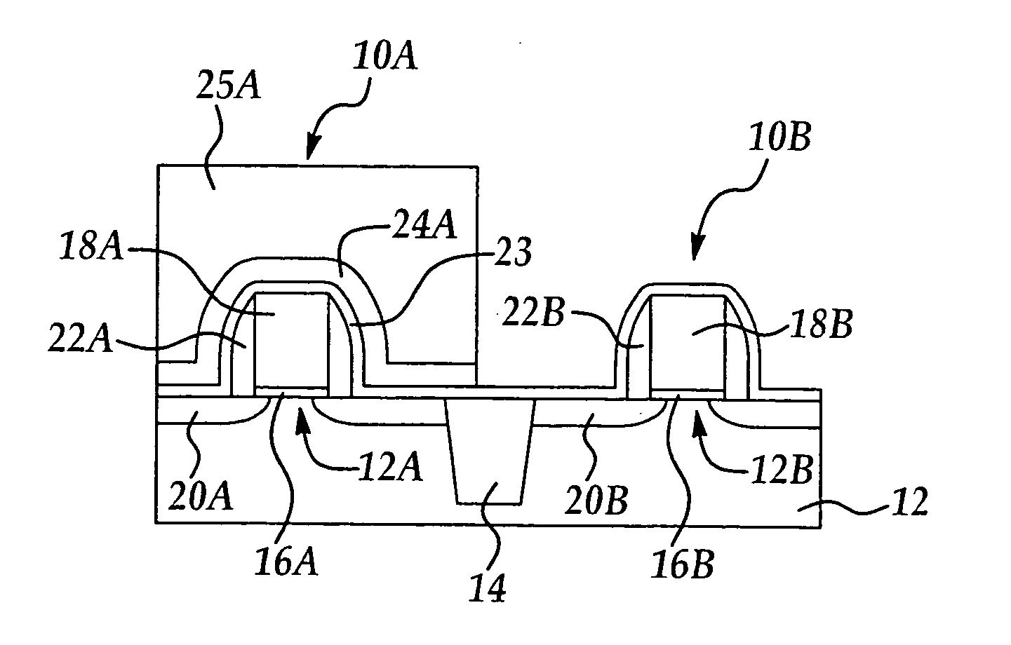
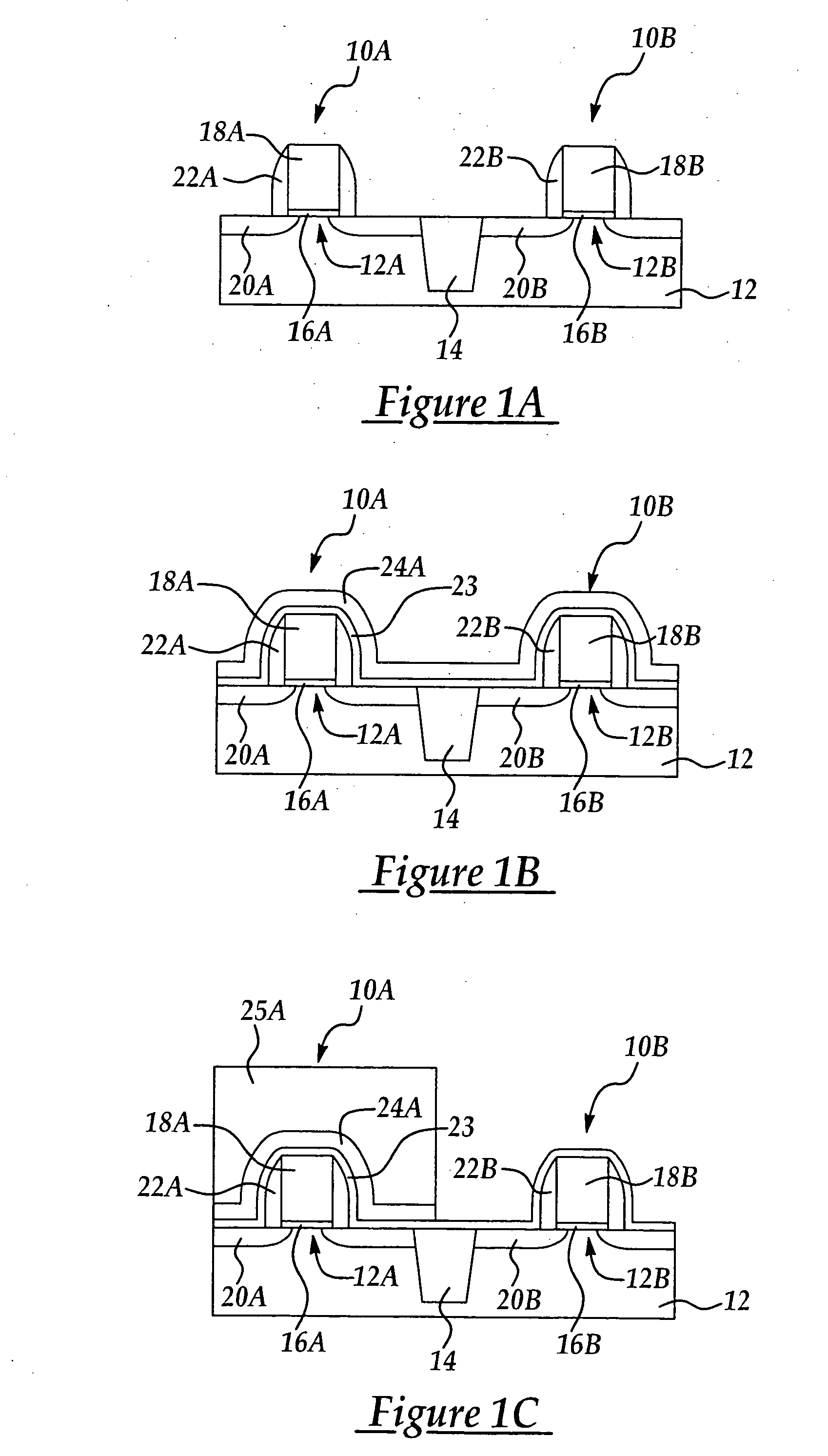
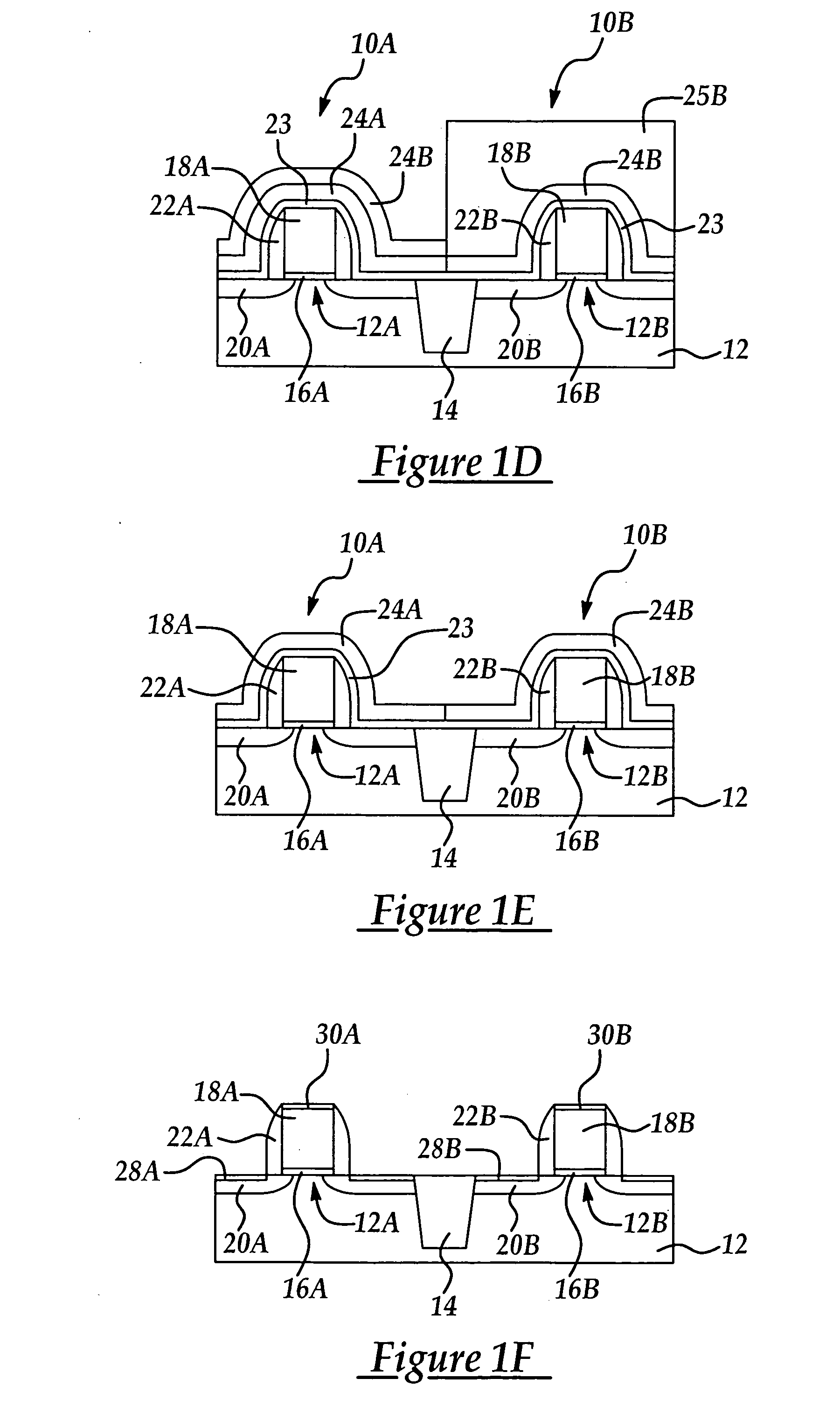
[0013] Although the method of the present invention is explained with reference to exemplary NMOS and PMOS devices, it will be appreciated that the method of the present invention may be applied to the formation of any MOSFET device where a stress level is controllably introduced into a charge carrier channel region by selective formation and subsequent removal of stressed dielectric layers overlying an NMOS and / or PMOS gate structure.

[0014] Referring to FIGS. 1A-1F in an exemplary embodiment of the method of the present invention, are shown cross-sectional schematic views of a portion of a semiconductor wafer during stages in production of CMOS structures including NMOS and PMOS devices 10A and 10B. For example, referring to FIG. 1A is shown a silicon substrate 12 including respective p-doped well regions 12A and n-doped well region 12B formed by conventional methods, for example a masking process followed by ion implantation and activation annealing. Formed by conventional proces...


PUM


Abstract

A strained channel MOSFET device with improved charge mobility and method for forming the same, the method including providing a first gate with a first semiconductor conductive type and second gate with a semiconductor conductive type on a substrate; forming a first strained layer with a first type of stress on said first gate; and, forming a second strained layer with a second type of stress on said second gate.

Description

FIELD OF THE INVENTION [0001] This invention generally relates to formation of MOSFET devices in integrated circuit manufacturing processes and more particularly to a method of selectively inducing stress (strain) into a MOSFET device to improve both electron and hole charge carrier mobility in respective MOSFET channel regions. BACKGROUND OF THE INVENTION [0002] Mechanical stresses are known to play a role in charge carrier mobility which affects Voltage threshold shifts. The effect of induced mechanical stresses, also referred to as strain in MOSFET device channel regions, on charge carrier mobility is believed to be influenced by complex physical processes related to acoustic and optical phonon scattering. [0003] Generally, manufacturing processes are known to introduce stress into the MOSFET device channel region. For example, stress is typically introduced into the channel region by formation of an overlying polysilicon gate structure and silicide formation processes. In additi...

Claims


Application Information

Patent Timeline
IPC IPC(8): H01L21/8238H01L29/76
CPCH01L29/7843H01L21/823807
Inventor CHEN, CHIEN-HAOCHEN, CHIA-LINHSU, JU-WANGLEE, TZE-LIANGCHEN, SHIH-CHANG
Owner TAIWAN SEMICON MFG CO LTD
Why Eureka
Try Eureka