

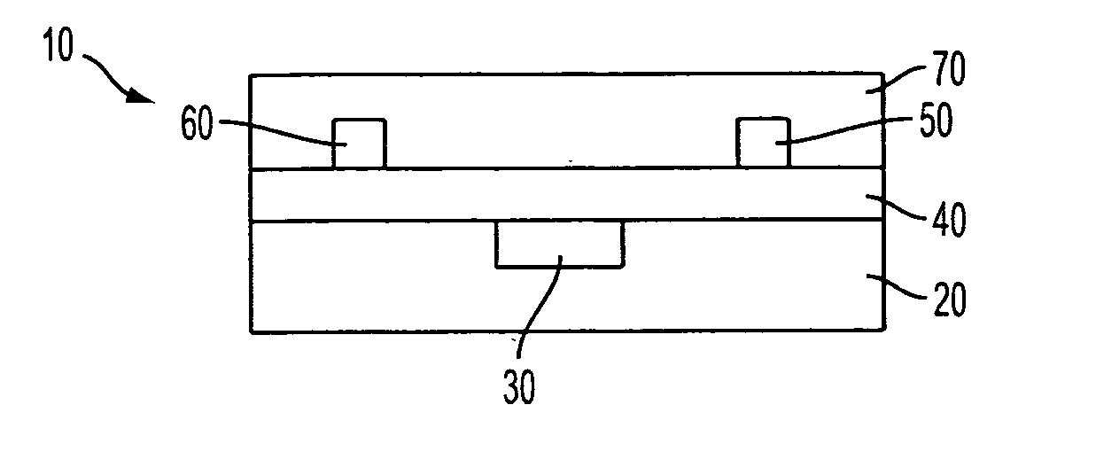
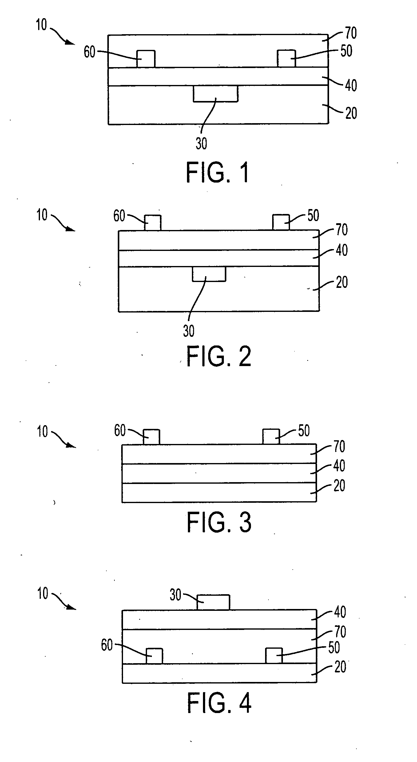
Organic thin-film transistors
a thin-film transistor and organic technology, applied in semiconductor devices, solid-state devices, thermoelectric devices, etc., can solve the problems of primarily high cost of silicon-based tft circuits, and the cost of tft circuits using current mainstream silicon technology may be too costly for some applications, so as to increase the charge carrier mobility of the semiconductor layer
- Summary
- Abstract
- Description
- Claims
- Application Information
AI Technical Summary
Benefits of technology
Problems solved by technology
Method used
Image

Examples
example 1
[0051] Doping the Semiconducting Polymer After Polymerization
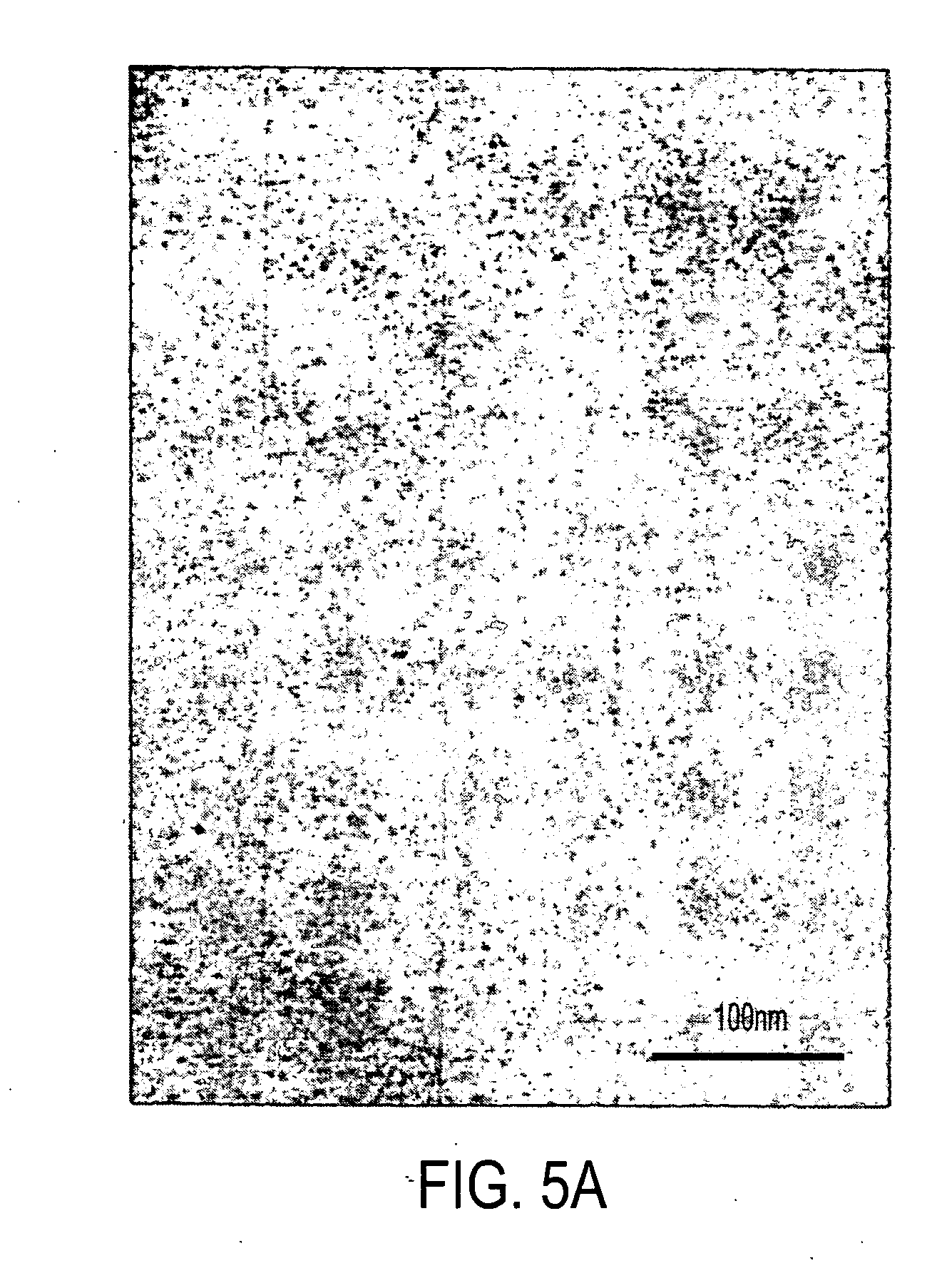
[0052] The semiconducting polymer was the same polythiophene as used in the Control Example and was synthesized with the active zinc methods. However, after polymerization occurred and before being applied onto the OTFTs, the semiconducting polymer was doped with FeCl3. The polymer was first dissolved in dichlorobenzene at a concentration of 0.5 percent by weight. Then FeCl3 dissolved in dichlorobenzene was added into above solution. The total FeCl3 was 0.2 percent of the polymer by weight of the polymer. The solution was then heated to about 80° C. and stirred for about 10 min. After cooling down to room temperature, the solution was filtrated with a 1.0 micrometer syringe filter before being spin coated onto the silicon substrate.
[0053] Device Fabrication and Evaluation
[0054] Top contact devices were fabricated as described in the Control Example except that the doped semiconducting polymer described above was used. U...
example 2
[0057] Doping the Semiconducting Polymer During Polymerization
[0058] The monomer, 5,5′-bis(3-dodecyl-2-thienyl)-2,2′-dithiophene, was synthesized using the same procedure as described in the Control Example. The polymerization of 5,5′-bis(3-dodecyl-2-thienyl)-2,2′-dithiophene was achieved by the FeCl3-mediated oxidative coupling reaction as follows:
[0059] A solution of 5,5′-bis(3-dodecyl-2-thienyl)-2,2′-dithiophene (0.50 gram, 0.75 mmol) in 7 milliliters of chloroform was added slowly over a period of about 10 minutes to a well stirred mixture of FeCl3 (0.40 gram, 2.47 mmol) in 3 milliliters of chloroform in a 50 milliliter round-bottomed flask in a dry atmosphere. The resultant mixture was heated at 50° C. for 1 hour, then 40° C. for 24 hours under a blanket of dry air. After the polymerization, the mixture was diluted with 20 milliliters of toluene and washed three times with water. The separated organic phase was stirred with 200 milliliters of 7.5 percent of an aqueous ammonia...
PUM
| Property | Measurement | Unit |
|---|---|---|
| Temperature | aaaaa | aaaaa |
| Temperature | aaaaa | aaaaa |
| Fraction | aaaaa | aaaaa |
Abstract
Description
Claims
Application Information