

Composition for dielectric thin film, metal oxide dielectric thin film using the same and preparation method thereof
a technology of metal oxide dielectric and thin film, applied in the direction of liquid/solution decomposition chemical coating, liquid organic insulator, coating, etc., can solve the problems of high vacuum deposition cost, high cost of equipment, deformation and damage of typical substrates
- Summary
- Abstract
- Description
- Claims
- Application Information
AI Technical Summary
Benefits of technology
Problems solved by technology
Method used
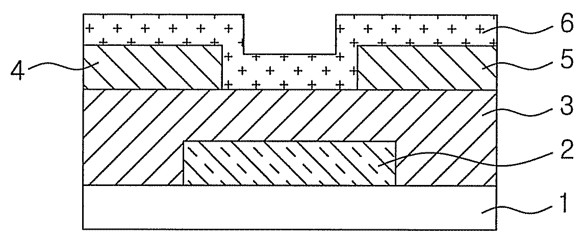
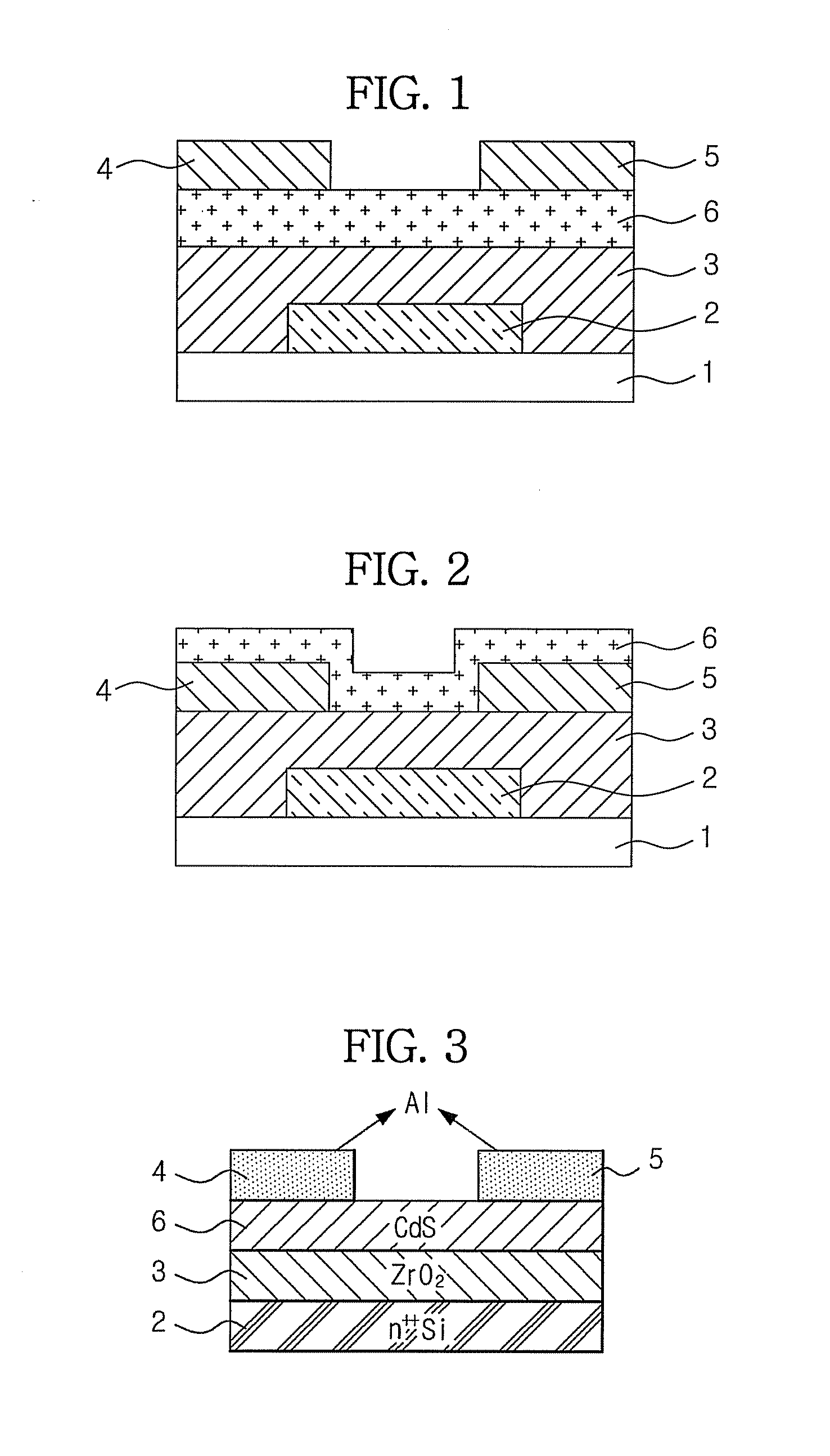
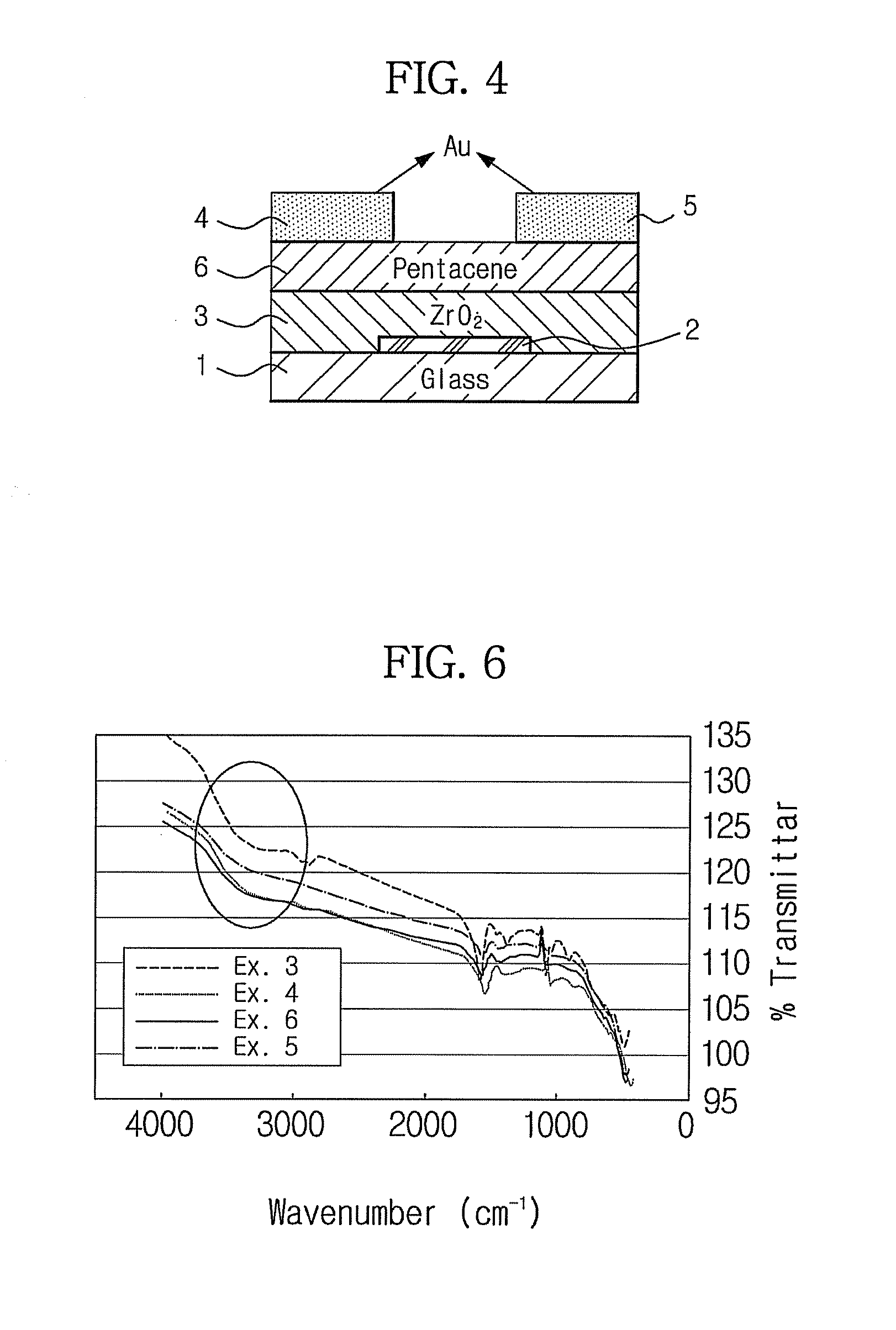
Image

Examples
example 1
Preparation of a Zirconium Oxide Dielectric Thin Film (1)
[0075]The composition prepared in Preparative Example 1, was applied onto a silicon wafer at room temperature through spin coating at 500 rpm for 30 seconds (sec). The composition was thermally treated at 100° C. for 1 min and then at 300° C. for 1 hour, in an ambient atmosphere, thus preparing a zirconium oxide (ZrO2) dielectric thin film with a thickness of about 416 Å.
example 2
Preparation of Zirconium Oxide Dielectric Thin Film (2)
[0076]A zirconium oxide dielectric thin film with a thickness of about 338 Å, was prepared in the same manner as in Example 1, with the exception that the thermal treatment was conducted at 100° C. for 1 min, at 200° C. for 5 min, and then at 400° C. for 30 min, in an ambient atmosphere.
example 3
Preparation of a Zirconium Oxide Dielectric Thin Film (3)
[0077]A zirconium oxide dielectric thin film was prepared in the same manner as in Example 1, with the exception that the thermal treatment was conducted at 100° C. for 1 min, and then at 300° C. for 5 min, in a nitrogen atmosphere.
PUM
| Property | Measurement | Unit |
|---|---|---|
| temperature | aaaaa | aaaaa |
| temperature | aaaaa | aaaaa |
| temperatures | aaaaa | aaaaa |
Abstract
Description
Claims
Application Information