Thin film transistor, method of forming the same and flat panel display device having the same

a thin film transistor and flat panel display technology, applied in transistors, solid-state devices, thermoelectric devices, etc., can solve the problems of deterioration of the driving characteristics of the tft, difficulty in increasing the operating speed, and reducing the charge mobility, so as to improve the charge mobility

Inactive Publication Date: 2010-06-17
RES & BUSINESS FOUND SUNGKYUNKWAN UNIV
View PDF3 Cites 31 Cited by
  • Summary
  • Abstract
  • Description
  • Claims
  • Application Information

AI Technical Summary

Benefits of technology

[0011]The present invention is directed to a TFT capable of dispersing an electric current by infiltrating a metal into source and drain regions when the TFT operates, thereby improving charge mobility, a method of forming the same, and a flat panel display device having the same.
[0012]The present invention is also directed to a TFT in which damage of the drain region caused by the excessive current density is prevented while the TFT is operating, thereby increasing the lifespan and improving performance, a method of forming the same, and a flat panel display device having the same.

Problems solved by technology

Therefore, in an LCD which uses a TFT having a channel formed of amorphous Si as a switching element, it is difficult to increase the operating speed.
Charges are concentrated in a local area A while moving to the drain region 7, and thus the extent to which charges are dispersed is increased in the local area A. As a result, there occurs a problem in that the charge mobility is decreased.
Also, the charge moving path CP1 becomes almost perpendicular in the drain region 7, and thus stress is continuously applied to the local area A. Consequently, as a time goes by, driving characteristics of the TFT deteriorate, leading to a short lifespan.

Method used


Image

  • Thin film transistor, method of forming the same and flat panel display device having the same
  • Thin film transistor, method of forming the same and flat panel display device having the same
  • Thin film transistor, method of forming the same and flat panel display device having the same

Examples


Embodiment Construction

[0032]Exemplary embodiments of the present invention will be described in detail below with reference to the accompanying drawings. While the present invention is shown and described in connection with exemplary embodiments thereof, it will be apparent to those skilled in the art that various modifications can be made without departing from the spirit and scope of the invention.

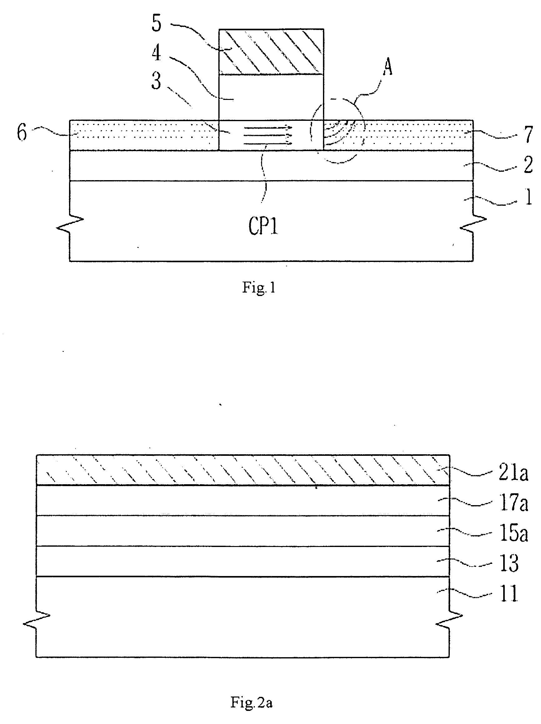
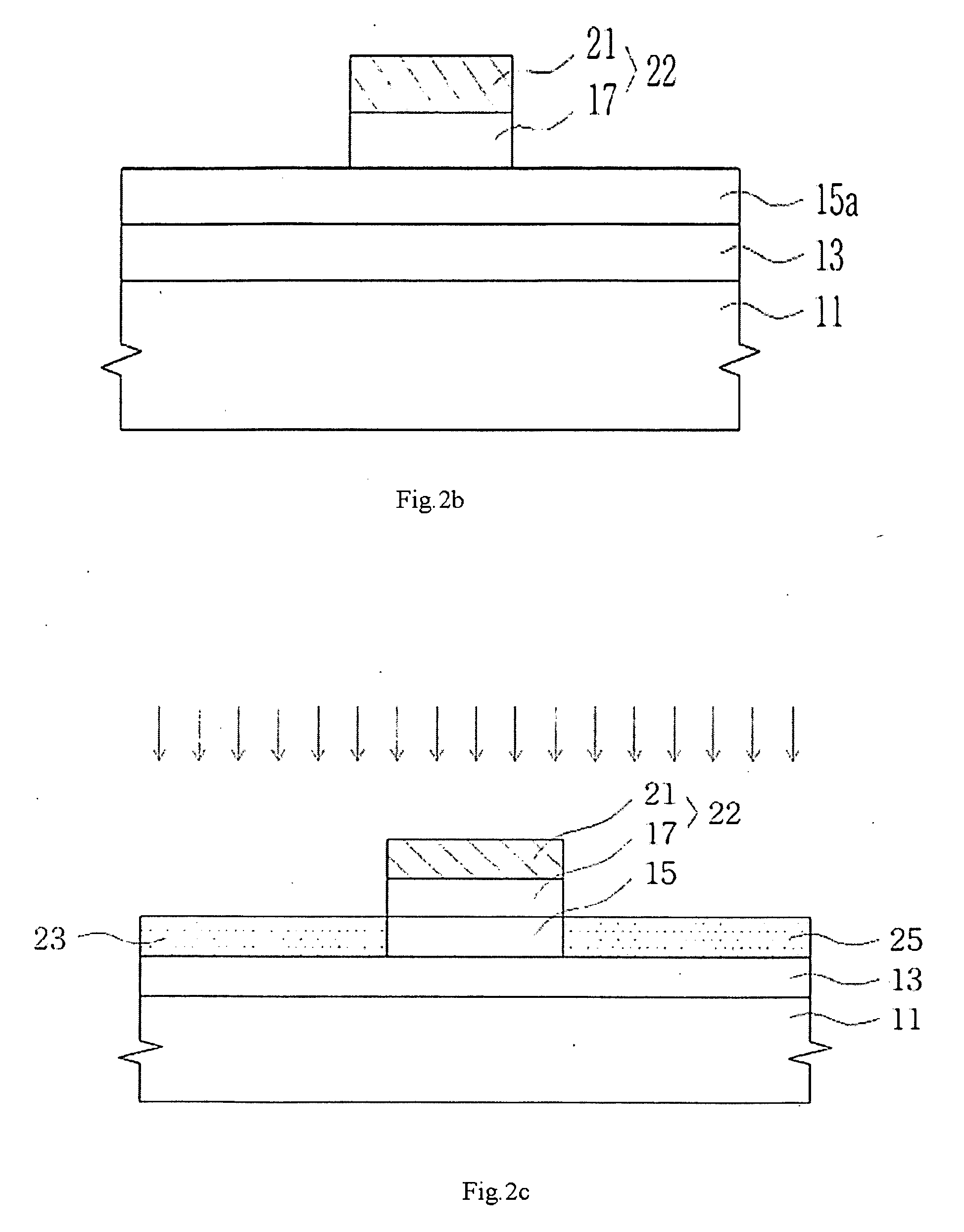
[0033]Hereinafter, a method of forming a TFT according to an exemplary embodiment of the present invention will be described in detail with reference to FIGS. 2A to 2H. FIGS. 2A to 2H are cross-sectional views illustrating a method of forming a TFT according to an exemplary embodiment of the present invention.

[0034]As shown in FIG. 2A, the TFT according to an exemplary embodiment of the present invention includes a buffer layer 13 formed on a glass substrate 11. The buffer layer 13 may be formed of a single layer of a silicon nitride (SiNx) layer or a silicon oxide (SiOx) layer or multi layers thereof. In the...


PUM


Abstract

A thin film transistor (TFT), a method of forming the same and a flat panel display device having the same are disclosed. The TFT includes a buffer layer and a semiconductor layer which are sequentially disposed on a substrate, a gate pattern including an insulating pattern and a gate electrode pattern which are sequentially disposed on the semiconductor layer, source and drain regions defining a portion of the semiconductor layer below the gate pattern as a channel area, formed by doping the semiconductor layer disposed at both sides of the gate pattern with impurities, and extending from both sides of the channel area, a passivation layer which covers the entire surface of the substrate having the gate pattern, a first metal electrode which penetrates a portion of the passivation layer disposed on the source area and a portion of the source region below the portion of the passivation layer to be electrically connected with the source region, and a second metal electrode which penetrates a portion of the passivation layer disposed on the drain area and a portion of the drain region below the portion of the passivation layer to be electrically connected with the drain region. According to the present invention, a metal is infiltrated into source and drain regions to disperse an electric current when a TFT operates, and thus charge mobility is improved, and damage of a drain region caused by the excessive current density is prevented, leading to the long lifespan and excellent performance.

Description

CROSS-REFERENCE TO RELATED APPLICATION[0001]This application claims priority to and the benefit of Korean Patent Application No. 10-2008-0127918, filed on Dec. 16, 2008, the disclosure of which is incorporated herein by reference in its entirety.BACKGROUND[0002]1. Field of the Invention[0003]The present invention relates to a thin film transistor (TFT), a method of forming the same, and a flat panel display device having the same, and more particularly, to a TFT capable of dispersing an electric current by infiltrating a metal into source and drain regions when the TFT operates, whereby charge mobility is improved, and damage of a drain region caused by the excessive current density is prevented, leading to the long lifespan and excellent performance, a method of forming the same, and a flat panel display device having the same.[0004]2. Discussion of Related Art[0005]A thin film transistor (TFT), which is a type of a field effect transistor (FET), is commonly not only applied to a s...

Claims


Application Information

Patent Timeline
Patent Type & Authority Applications(United States)
IPC IPC(8): H01L29/786H01L21/336H01L51/52
CPCH01L27/3262H01L29/78606H01L29/66757H01L29/41733H10K59/1213H01L29/78618
Inventor CHOI, BYOUNG DEOGYI, JUN SINJUNG, SUNG WOOKJANG, KYUNG SOOCHO, JAE HYUN
Owner RES & BUSINESS FOUND SUNGKYUNKWAN UNIV
Why Eureka
Try Eureka