Image display and Its control method

a technology of image display and control method, which is applied in the field of image display apparatus, can solve the problems of reducing the aperture of the pixel, lowering and difficulty in manufacturing process, so as to reduce the luminance variation of light emission and increase the quality of the displayed image

Active Publication Date: 2005-09-22
HANNSTAR DISPLAY CORPORATION
View PDF3 Cites 478 Cited by
  • Summary
  • Abstract
  • Description
  • Claims
  • Application Information

AI Technical Summary

Benefits of technology

[0022] It is an object of the present invention to provide an image display apparatus for suppressing light emission luminance variations of respective pixel display elements to increase the quality of the displayed image.

Problems solved by technology

As described above, the conventional image display apparatus is problematic in that even when identical gradation pixel data, i.e., signal voltages, are written, the current control elements emit light at different luminances, lowering the quality of the displayed image.
Therefore, the aperture of the pixel is reduced, resulting in manufacturing process difficulty.

Method used


Image

  • Image display and Its control method
  • Image display and Its control method
  • Image display and Its control method

Examples


first embodiment

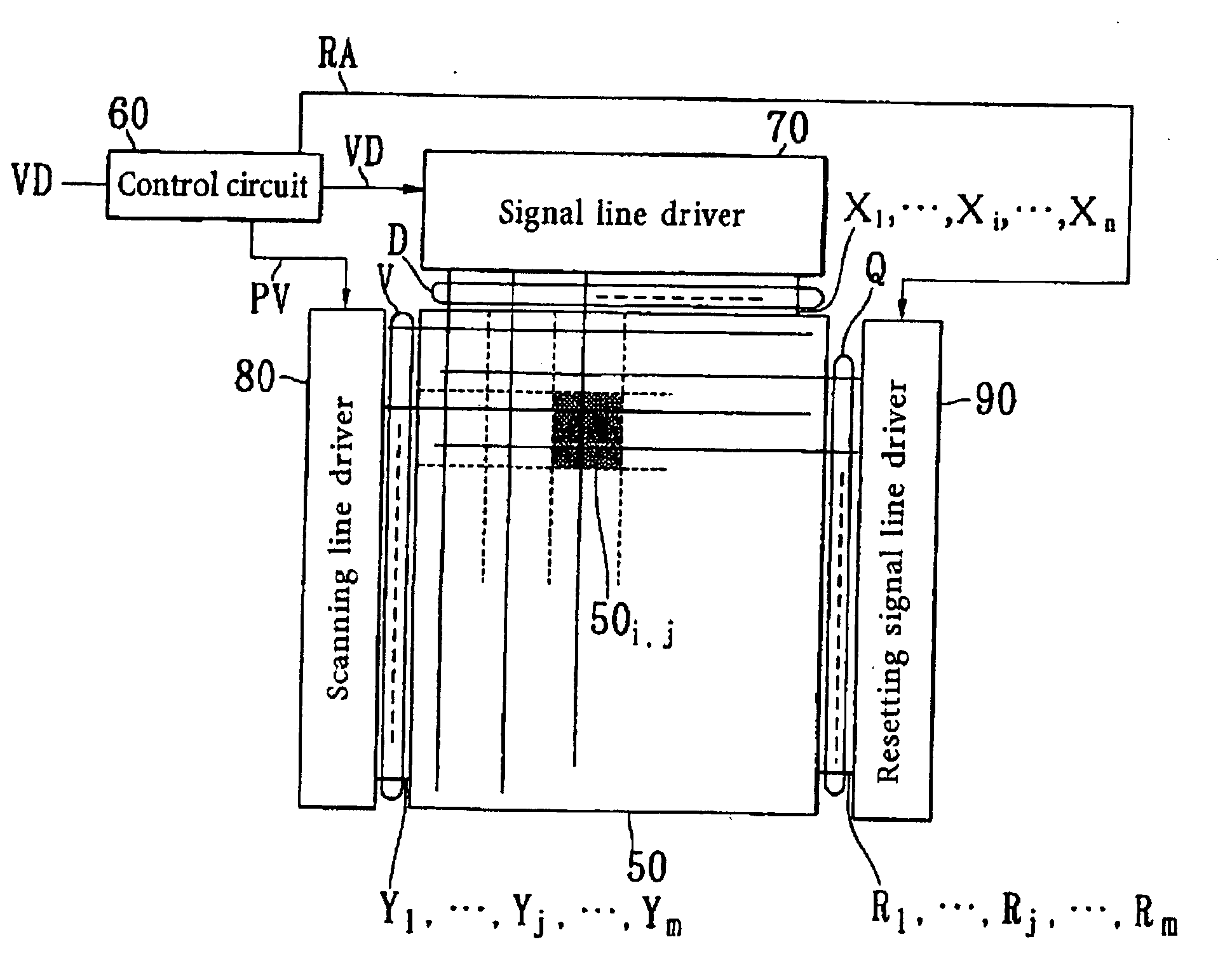
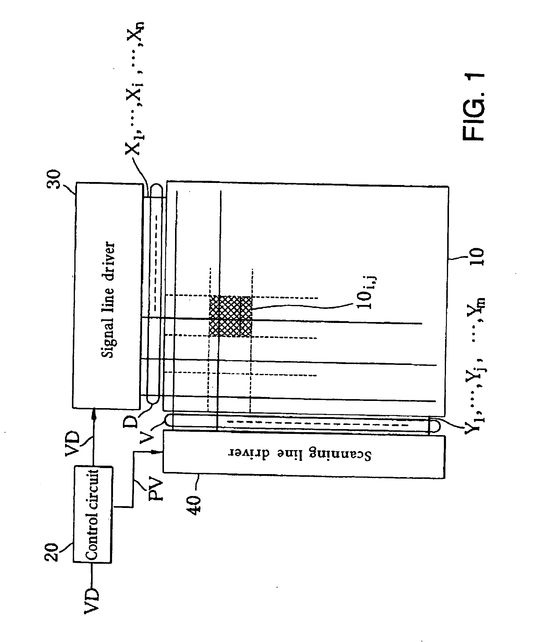
[0086]FIG. 6 is a block diagram of an electric arrangement of an image display apparatus according to a first embodiment of the present invention.

[0087] The image display apparatus comprises display panel 50, control circuit 60, signal line driver 70, scanning line driver 80, and resetting signal line driver 90. Display panel 50 comprises an organic EL display, for example, and has a plurality of signal lines X1, . . . , Xi, . . . , Xn to which gradation pixel data D are applied, a plurality of scanning line Y1, . . . , Yj, . . . , Ym to which scanning signals V are applied, a plurality of resetting signal lines R1, . . . , Rj, . . . , Rm to which resetting signals Q are applied, and a plurality of pixels 50i,j (i=1, 2, . . . , n, j=1, 2, . . . , m) disposed at points of intersection between signal lines X1, . . . , Xi, . . . , Xn and scanning lines Y1, . . . , Yj, . . . , Ym. Of pixels 50i,j, those pixels on scanning lines that are selected by scanning signals V are supplied with ...

second embodiment

[0106]FIG. 16 is a block diagram of an electric arrangement of an image display apparatus according to a second embodiment of the present invention. Common reference characters are assigned to those elements in FIG. 16 which are common to the elements shown in FIG. 6 illustrating the first embodiment.

[0107] The image display apparatus according to the present embodiment has control circuit 60B having a different function and display panel 50B having a different arrangement, instead of control circuit 60 and display panel 50 shown in FIG. 6. Control circuit 60B supplies resetting control signal RB having a different timing from resetting control signal RA shown in FIG. 6 to resetting signal line driver 90. Display panel 50B has pixels 50Bi,j having a different arrangement, instead of pixels 50i,j shown in FIG. 6. Other details are identical to those shown in FIG. 6.

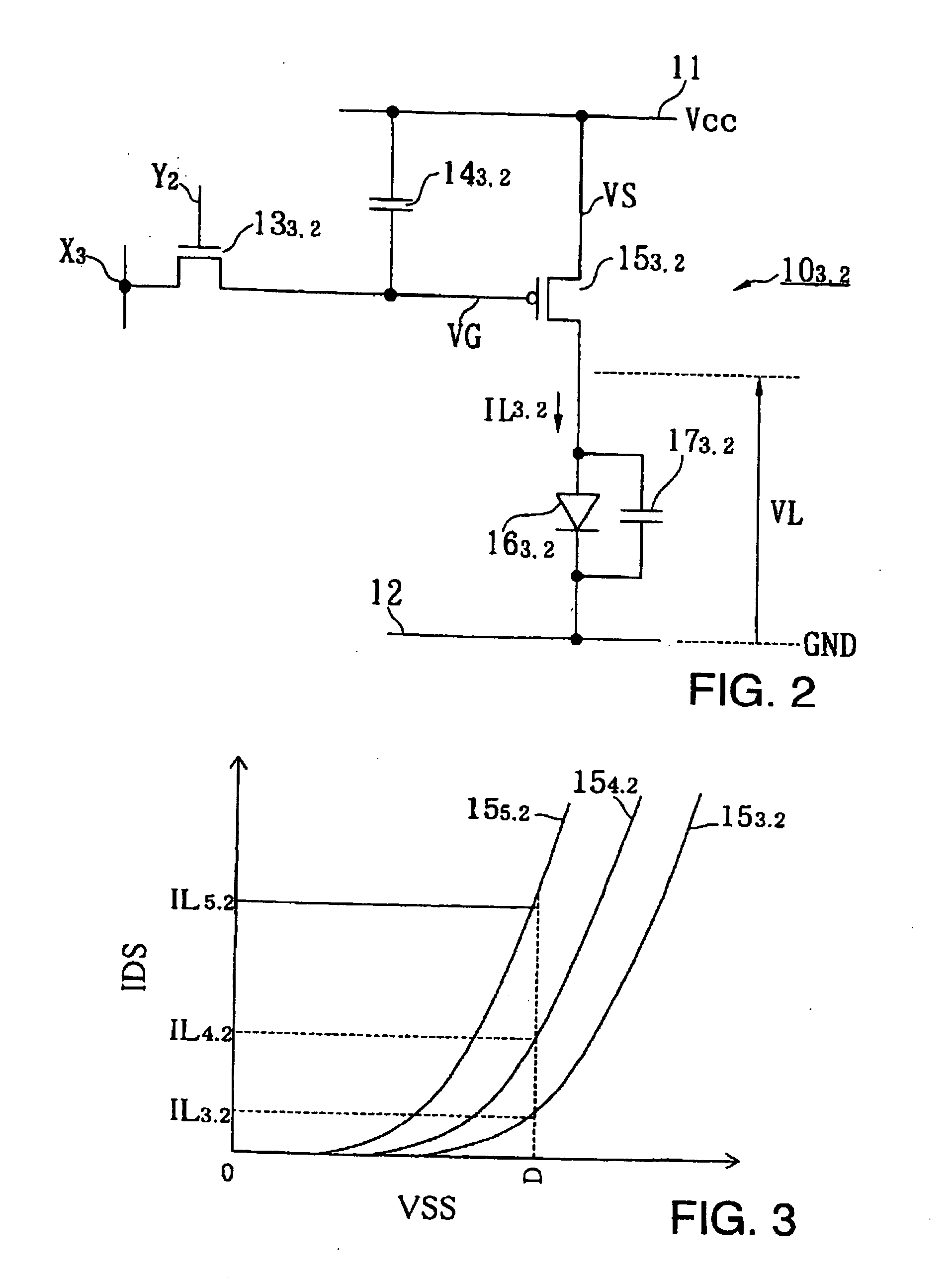
[0108]FIG. 17 is a circuit diagram of an electric arrangement of pixel 50Bi,j (e.g., i=3, j=2) in the image display ap...

third embodiment

[0113]FIG. 19 is a block diagram of an electric arrangement of an image display apparatus according to a third embodiment of the present invention. Common reference characters are assigned to those elements in FIG. 19 which are common to the elements shown in FIG. 6 according to the first embodiment.

[0114] The image display apparatus shown in FIG. 19 has control circuit 60C having a different function and display panel 50C having a different arrangement, instead of control circuit 60 and display panel 50 in the image display apparatus shown in FIG. 6. Resetting signal line driver 90 shown in FIG. 6 is dispensed with. Control circuit 60C supplies image input signal VD having a different timing from control circuit 60 to signal line driver 70. Display panel 50C has pixels 50Ci,j having a different arrangement, instead of pixels 50i,j shown in FIG. 6. Other details are identical to those of the image display apparatus shown in FIG. 6.

[0115]FIG. 20 is a circuit diagram of an electric ...


PUM


Abstract

An image display apparatus comprises a pixel having a drive transistor and a pixel display element which are connected in series between a first power line and a second power line, a holding capacitor connected to a gate electrode of the drive transistor, and a selection transistor connected between a signal line and the gate electrode of the drive transistor. When the selection transistor is turned on, gradation pixel data is written in the holding capacitor from the signal line. The charge of gradation pixel data written in the holding capacitor is discharged for a certain period through the drive transistor, thereafter the charge of the gradation pixel data stored in the holding capacitor is held by floating the gate electrode of the drive transistor.

Description

TECHNICAL FIELD [0001] The present invention relates to an image display apparatus and a control method for use with such an image display apparatus, and more particularly to an image display apparatus using pixel display elements that are current-driven based on gradation pixel data, such as an organic EL (electroluminescence) display, for example, a control method for use with such an image display apparatus, a drive circuit for causing current control elements such as organic EL elements to emit light in such an image display apparatus, and a drive method for the drive circuit. BACKGROUND ART [0002] Image display apparatus using pixel display elements that are driven under current control, such as organic EL displays or the like, have drive circuits associated with respective pixels of driving those pixel display elements, i.e., current control elements. The drive circuits are arrayed two-dimensionally in association with the respective pixels, making up the image display apparat...

Claims


Application Information

Patent Timeline
Patent Type & Authority Applications(United States)
IPC IPC(8): G09G3/32
CPCG09G3/3233G09G3/3241G09G2300/0465G09G2300/0819G09G2320/043G09G2300/0861G09G2310/0251G09G2310/0254G09G2310/0256G09G2300/0842
Inventor SASAKI, ISAOIGUCHI, KOICHI
Owner HANNSTAR DISPLAY CORPORATION
Why Eureka
Try Eureka