Tray for storing and transporting semi-conductor and other microelectronic components

a technology for semi-conductor and other microelectronic components, applied in the direction of metal-working machine components, manufacturing tools, instruments, etc., can solve the problems of less tolerances, less storage space, and more difficult handling of microelectronic components, so as to minimize the possibility of damage, minimize the sliding and rattling of components in the pocket, and minimize the effect of potential damag

Inactive Publication Date: 2005-09-29
ENTEGRIS INC
View PDF3 Cites 5 Cited by
  • Summary
  • Abstract
  • Description
  • Claims
  • Application Information

AI Technical Summary

Benefits of technology

[0010] An advantage and feature of particular embodiments is that a chip tray is provided that is capable of securing different size components, particularly components with different heights in the pockets of the chip tray.
[0011] A further advantage and feature of the invention is that the components are gently secured in the pockets of the chip tray and sliding and rattling of the components in the pocket is minimized or eliminated.
[0012] A further advantage and feature of the invention is that the foam material can be static dissipative to minimize potential for damage from static electricity.

Problems solved by technology

As microelectronic components have become smaller they have become more difficult to handle.
In particular some microelectronic components have become so small that their overall size is less than the tolerances that can reasonably be attained in the manufacturing of chip trays.
Thus it has become prohibitively difficult and expensive to manufacture form fitting chip trays with tight fitting lids that are sufficiently close to the microelectronic components to keep them from shifting while the chip tray is in transit.

Method used


Image

  • Tray for storing and transporting semi-conductor and other microelectronic components
  • Tray for storing and transporting semi-conductor and other microelectronic components
  • Tray for storing and transporting semi-conductor and other microelectronic components

Examples


Embodiment Construction

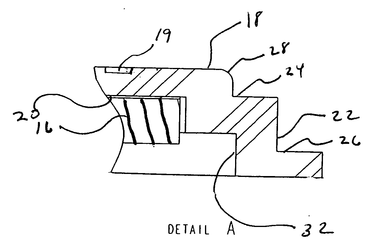
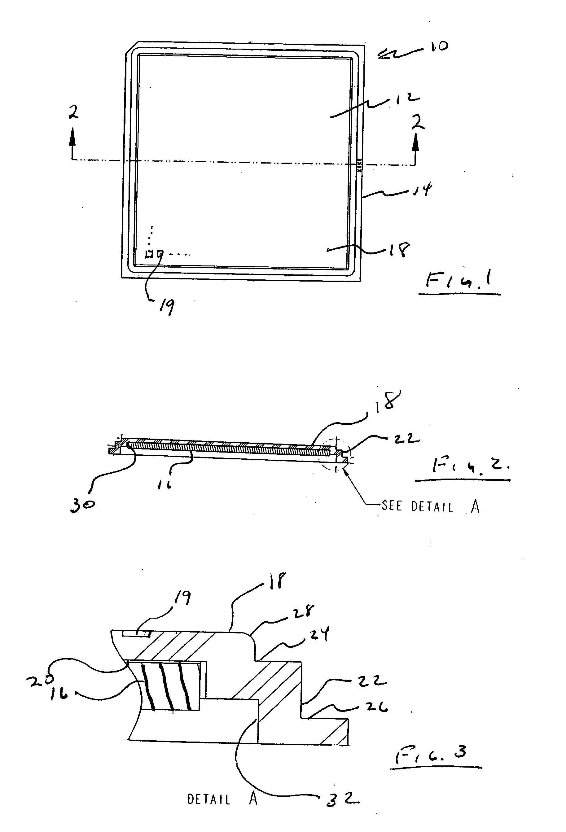
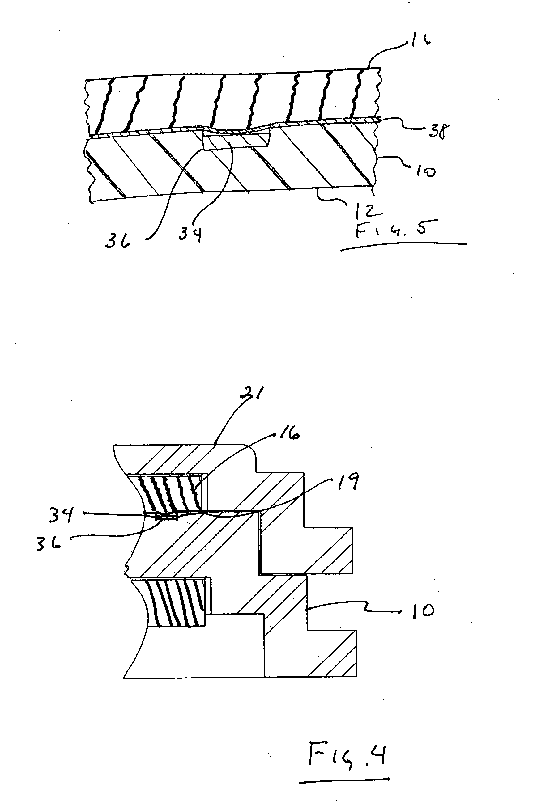
[0020] The microelectronics transport tray 10 of the present invention as depicted in FIGS. 1-3 generally includes a body portion or plate 12, a rail or plate surround 14 and a resiliently compressible sheet member 16.

[0021] Plate 12 generally includes a top surface 18 and a bottom surface 20. Plate 12 is depicted herein as a square shape but plate 12 may take any shape desired. Top surface 18 will generally include a plurality or multiplicity of cavities 19 which are shaped and sized to accept a particular microelectronic component and that have a matrixical arrangement on the top surface. The microelectronics transport tray 10 as described in this application is exemplary. The present invention may be utilized with other stackable microelectronics transport tray 10 or lid 21. The use of the invention with a lid will be readily apparent to those skilled in the art.

[0022] Plate 12 is bound on its perimeter by plate support 14. Plate surround 14 generally supports plate 12 in such ...


PUM

PropertyMeasurementUnit
thickaaaaaaaaaa
thickaaaaaaaaaa
thickaaaaaaaaaa

Abstract

A chip tray of the present invention includes on its underside a resilient sheet member that resiliently retains microelectronic components in the chip tray below by pressing gently but firmly down on the microelectronic components and the separators between cavities that contain the components.

Description

FIELD OF THE INVENTION [0001] The present invention relates to a tray for storing and transporting miniature electronic components, commonly known as a chip trays. BACKGROUND OF THE INVENTION [0002] Microelectronic components go through many processing steps during their manufacturer. Microelectronic components have been getting smaller and smaller as time goes by. Commonly, in fabricating facilities microelectronic components such as chips and other components are transported in trays. Generally the trays have numerous form fitting compartments so that numerous microelectronic components can be handled and transported at one time. Generally, so called chip trays are designed to be stackable so that multiple trays can be transported. Thus one chip tray forms the cover for the chip tray immediately below it. When a desired number of trays are stacked for transport a dedicated cover is applied to the top tray to keep the components covered and secure. [0003] As microelectronic compone...

Claims


Application Information

Patent Timeline
Patent Type & Authority Applications(United States)
IPC IPC(8): G01R1/00H01L21/673
CPCH01L21/67336Y10T29/53174Y10T29/53091
Inventor NIGG, JAMES R.HARRISON, WILL D.
Owner ENTEGRIS INC
Why Eureka
Try Eureka