
Diode junction poly fuse

a poly fuse and diode junction technology, applied in the direction of electrical equipment, semiconductor devices, semiconductor/solid-state device details, etc., can solve the problems of blowing the fuse, complicated processing steps, and expensive laser equipment,

Inactive Publication Date: 2005-09-29
TAIWAN SEMICON MFG CO LTD
View PDF3 Cites 74 Cited by
  • Summary
  • Abstract
  • Description
  • Claims
  • Application Information

AI Technical Summary

Benefits of technology

[0008] These and other problems are generally solved or circumvented, and technical advantages are generally achiev...

Problems solved by technology

If a memory circuit is found to be defective or is not needed, the fuse may be blown thereby activating or deactivating the redundant memory cells.
The use of the laser, however, requires complicated processing steps and expensive laser equipment.
Because the p-n junction diode does not allow the current to flow in this configuration, the current flows through the silicided layer.
The current crowding in the silicide layer over the p-n junction causes silicide migration or melting of the link, thereby blowing the fuse.

Method used


Image

  • Diode junction poly fuse
  • Diode junction poly fuse
  • Diode junction poly fuse

Examples


Embodiment Construction

[0023] The making and using of the presently preferred embodiments are discussed in detail below. It should be appreciated, however, that the present invention provides many applicable inventive concepts that can be embodied in a wide variety of specific contexts. The specific embodiments discussed are merely illustrative of specific ways to make and use the invention, and do not limit the scope of the invention.

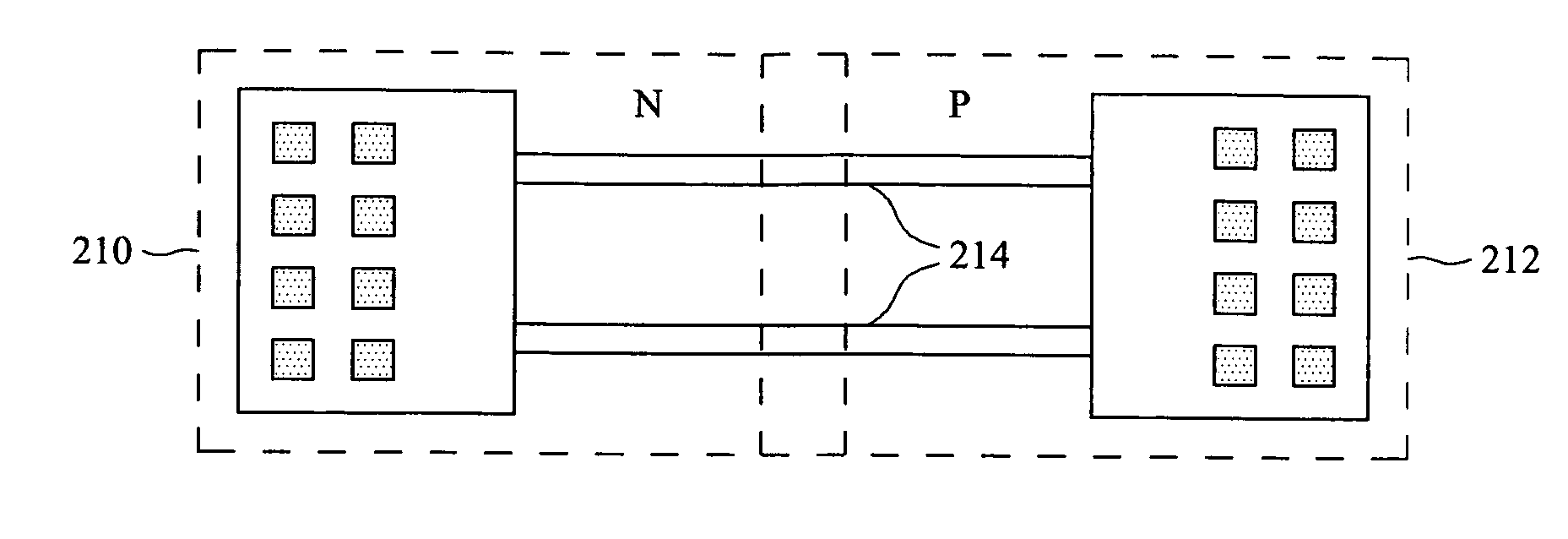
[0024] The present invention will be described with respect to preferred embodiments in a specific context, namely an electrical fuse having one or more links, each link having one or more p-n junction diodes. The cathode and anode are symmetrical and approximately the same size, and the links are straight. The present invention, however, may also be applied to other fuse structures having varying shapes, sizes, and configurations.

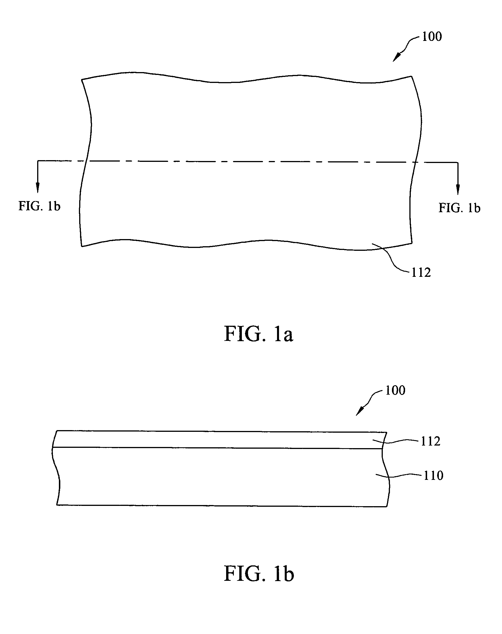
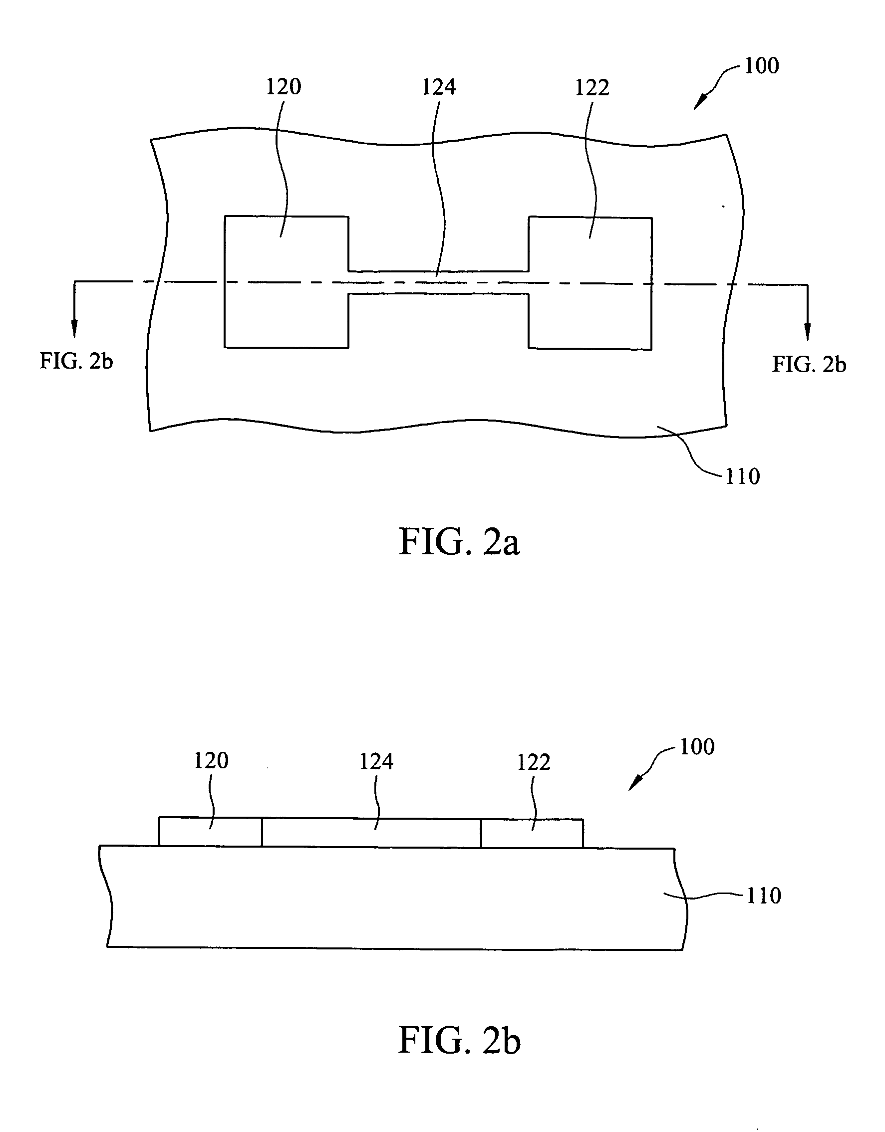
[0025]FIGS. 1a-5b illustrate a method for forming a single-link fuse structure in accordance with one embodiment of the present invention. The m...


PUM


Abstract

System and method for providing an electrical fuse having a p-n junction diode. A preferred embodiment comprises a cathode, an anode, and one or more links formed between the cathode and the anode. The cathode and the portion of the cathode adjoining the link are doped with a first impurity, preferably a p-type impurity. The anode and the portion of the link adjoining the anode are doped with a second impurity, preferably an n-type impurity. The junction of the first impurity and the second impurity in the link forms a p-n junction diode. A conductive layer, such as a silicide layer, is formed over the p-n junction diodes. In an alternative embodiment, a plurality of p-n junction diodes may be formed in each link. One or more contacts may be formed to provide electrical contact to the cathode and the anode.

Description

TECHNICAL FIELD [0001] The present invention relates generally to a system and method for an electrical fuse, and more particularly to a system and method for an electrical fuse for use in semiconductor devices. BACKGROUND [0002] Fuses are commonly used in integrated circuits to provide redundancy and programming capabilities. To increase yield in integrated circuits such as memory chips, it is common to include redundant memory cells on the memory chips. If a memory circuit is found to be defective or is not needed, the fuse may be blown thereby activating or deactivating the redundant memory cells. Another common practice is to utilize fuses to program or customize integrated circuits for a particular application or customer. In this manner, the same chip may be produced and customized for individual customers by programming the fuses after fabrication, thereby reducing the fabrication costs. [0003] Typically, fuses comprise a conductive link that may be blown or ruptured to preve...

Claims


Application Information

Patent Timeline
IPC IPC(8): H01L21/768H01L21/82H01L23/525H01L29/00H01L29/36H01L29/74H01L29/861
CPCH01L23/5256H01L2924/0002H01L2924/00
Inventor WU, SHIEN-YANGCHEN, SHI-BAI
Owner TAIWAN SEMICON MFG CO LTD
Features
  • Generate Ideas
  • Intellectual Property
  • Life Sciences
  • Materials
  • Tech Scout
  • Unparalleled Data Quality
  • Higher Quality Content
  • 60% Fewer Hallucinations
Learn More