Lead on chip semiconductor package

a lead frame and chip technology, applied in semiconductor devices, semiconductor/solid-state device details, electrical equipment, etc., can solve problems such as frame and chip creating various problems, affecting the performance of semiconductor chips, and affecting the quality of semiconductor chips

Inactive Publication Date: 2005-09-29
SAMSUNG ELECTRONICS CO LTD
View PDF14 Cites 2 Cited by
  • Summary
  • Abstract
  • Description
  • Claims
  • Application Information

AI Technical Summary

Problems solved by technology

The layer of adhesive material between the lead frame and the chip creates various problems.
For example, if pressure is applied to secure the adhesive material to the chip and to the frame, this can damage the semiconductor chip.
Another potential problem is created by the fact that the layer of adhesive material separates the lead frame from the semiconductor chip.
This separation can create a space into which packaging material can flow, causing potential failure sites.

Method used


Image

  • Lead on chip semiconductor package
  • Lead on chip semiconductor package
  • Lead on chip semiconductor package

Examples


Embodiment Construction

[0021] The present invention will now be described more fully hereinafter with reference to the accompanying drawings, in which preferred embodiments of the invention are shown. This invention may, however, be embodied in different forms and should not be construed as limited to the embodiments set forth herein. Rather, these embodiments are provided to convey the scope of the invention to those skilled in the art.

[0022] It is noted that the figures are not drawn to scale. Rather, for simplicity and clarity of illustration, the dimensions of some of the elements are exaggerated for clarity. It is also noted that well-known structures and processes have not been described or illustrated to avoid obscuring the essence of the present invention.

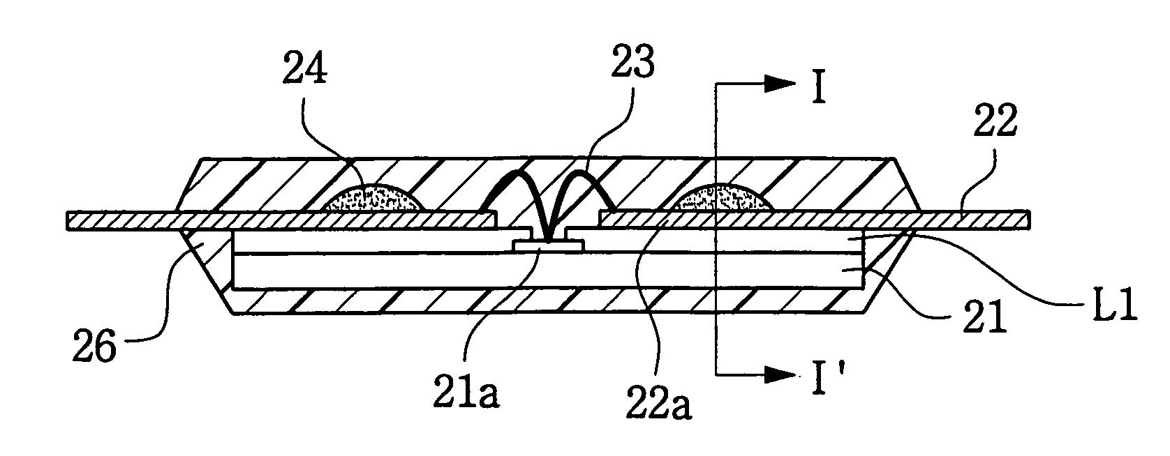
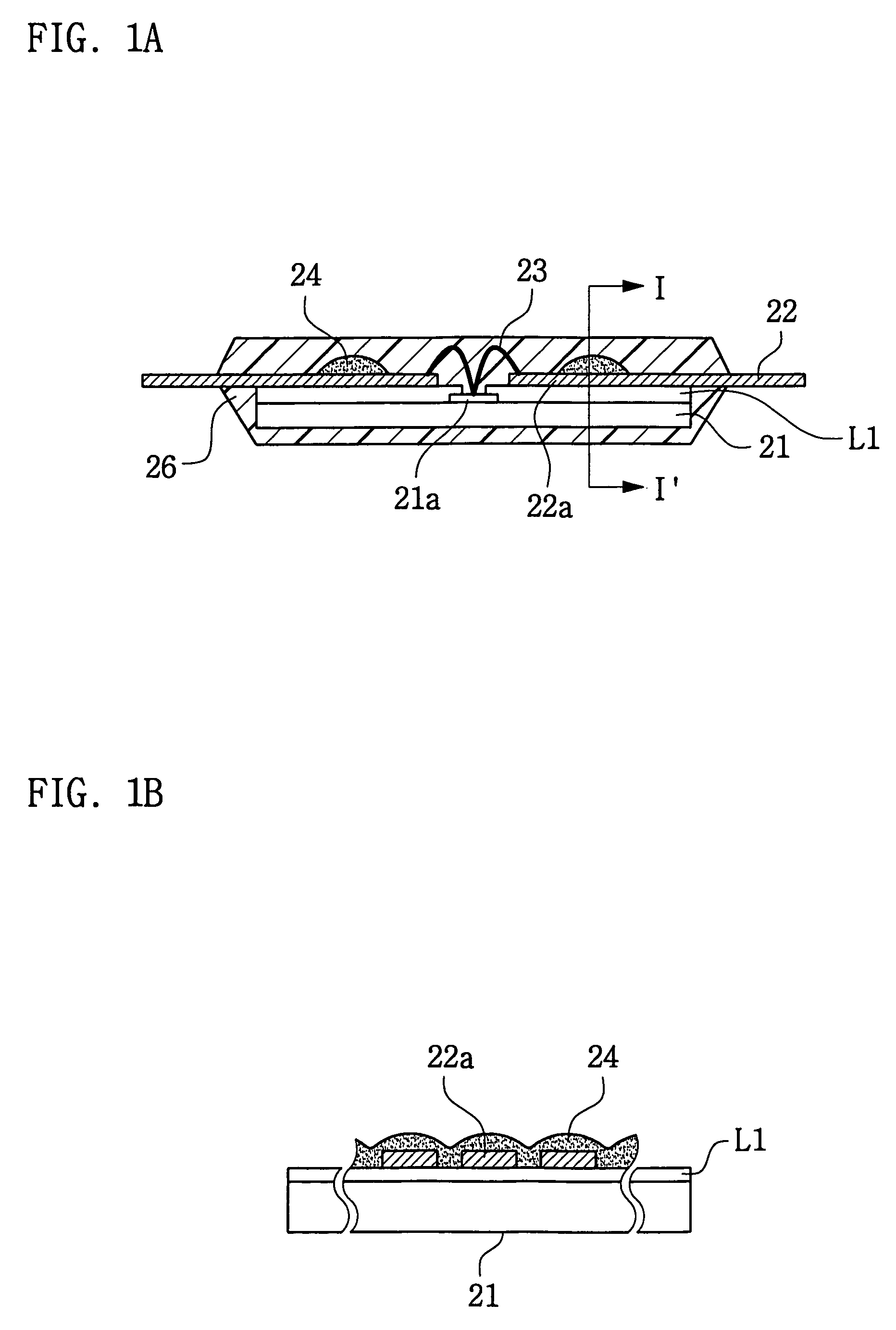
[0023]FIG. 1A is a cross section view of a Lead-on-chip (LOC) semiconductor package that incorporates a first embodiment of the present invention. FIG. 1B is a cross section view taken along line I-I′ in FIG. 1A.

[0024] The LOC package shown in...


PUM


Abstract

The present invention provides an LOC package wherein the lead frame is in direct contact with the semiconductor device. The lead frame, which includes openings, is positioned directly on the semiconductor device. An adhesive material is applied in the opening in the lead frame. This adhesive material contacts both the lead frame and the semiconductor device. The lead frame is therefore securely held to the semiconductor device. Wires can then be bonded to contact pads on the semiconductor device and to the lead frame.

Description

CROSS-REFERENCE TO RELATED APPLICATIONS [0001] This U.S. non-provisional patent application claims priority under 35 U.S.C. § 119 of Korean Patent Application P2004-0019664 filed Mar. 23, 2004 and Korean Patent Application No. P2004-0093481 filed Nov. 16, 2004, the entire contents of which are hereby incorporated by reference. FIELD OF THE INVENTION [0002] The present invention relates to packaging semiconductor devices and more particularly to packaging semiconductor devices using a lead frame. BACKGROUND OF THE INVENTION [0003] There are a wide variety of packaging technologies that have been used for semiconductor devices. One of the widely used packaging technologies is termed Lead On Chip (LOC). [0004] In LOC packaging a lead frame is positioned near the semiconductor device and wires are then bonded to pads on the chip and to the lead frame. Generally the wires are bonded to pads on the chip and to the lead frame using ultrasonic wire bonding technology. After the lead frame i...

Claims


Application Information

Patent Timeline
Patent Type & Authority Applications(United States)
IPC IPC(8): H01L23/495
CPCH01L23/4951H01L2924/00014H01L24/06H01L2224/04042H01L2224/05599H01L2224/06136H01L2224/32014H01L2224/32245H01L2224/48091H01L2224/48247H01L2224/4826H01L2224/49171H01L2224/73215H01L2224/85399H01L2224/92247H01L2924/01005H01L2924/01006H01L2924/01015H01L2924/01082H01L2924/14H01L23/49513H01L24/49H01L2224/05554H01L2924/01033H01L24/32H01L24/48H01L2224/45099H01L2924/00H01L2924/00012H01L23/28
Inventor LEE, SANG-HYEOPOH, SE-YONGKIM, JING-HOLEE, CHAN-SUKKWAK, MIN-KEUNYOON, SUNG-HWANNAM, TAE-DUK
Owner SAMSUNG ELECTRONICS CO LTD
Why Eureka
Try Eureka