

Scanning probe microscope
a probe microscope and scanning probe technology, applied in the direction of mechanical measurement arrangements, mechanical roughness/irregularity measurements, instruments, etc., can solve the problems of erroneously determining that a sample that is out of spec is within spec, prolonging the time required for evaluation, etc., and achieve the effect of easy determination
- Summary
- Abstract
- Description
- Claims
- Application Information
AI Technical Summary
Benefits of technology
Problems solved by technology
Method used
Image

Examples
first embodiment
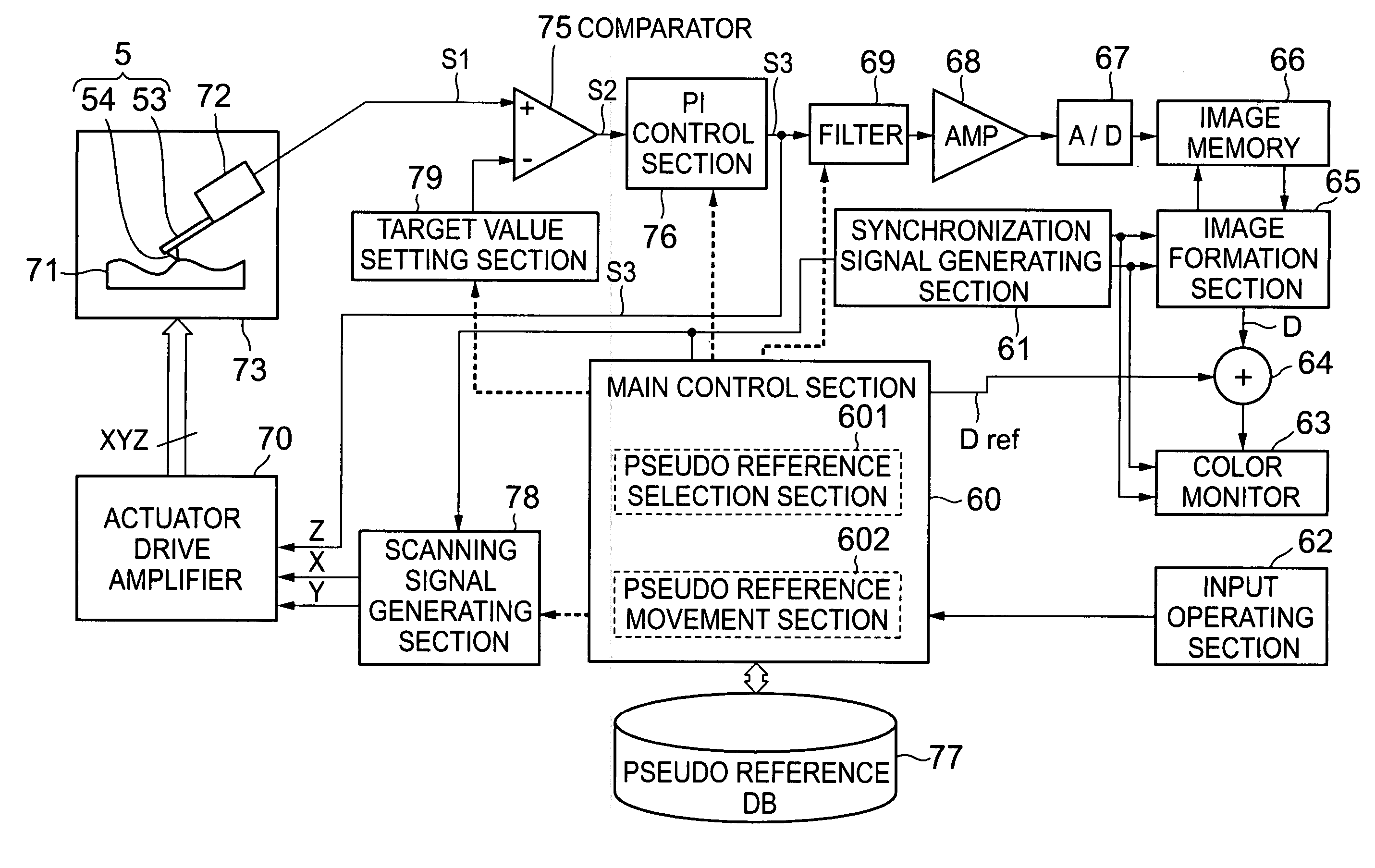
[0032] Preferred embodiments of the present invention will be described in detail in the following with reference to the drawings. FIG. 1 is a block diagram showing the structure of a scanning probe microscope that adopts the present invention. In the drawing, a scanning probe 5 has a probe needle 54 attached to a free end of a cantilever 53 positioned so as to be opposite an observation surface of a sample 71. Strain of the cantilever 53 is detected by a detection section 72 and input to the non-inverting input terminal (+) of a comparator 75 as a strain signal S1 representing a gap between the sample surface and the probe needle 54. A target value signal relating to strain amount of the probe needle 53 is input to the inverting input terminal (−) of the comparator 75 from a target value setting section 79.
[0033] An error signal S2 output from the comparator 75 is input to a proportional integral (PI) control section 76, and a signal that is a combination of the error signal S2 and...
second embodiment
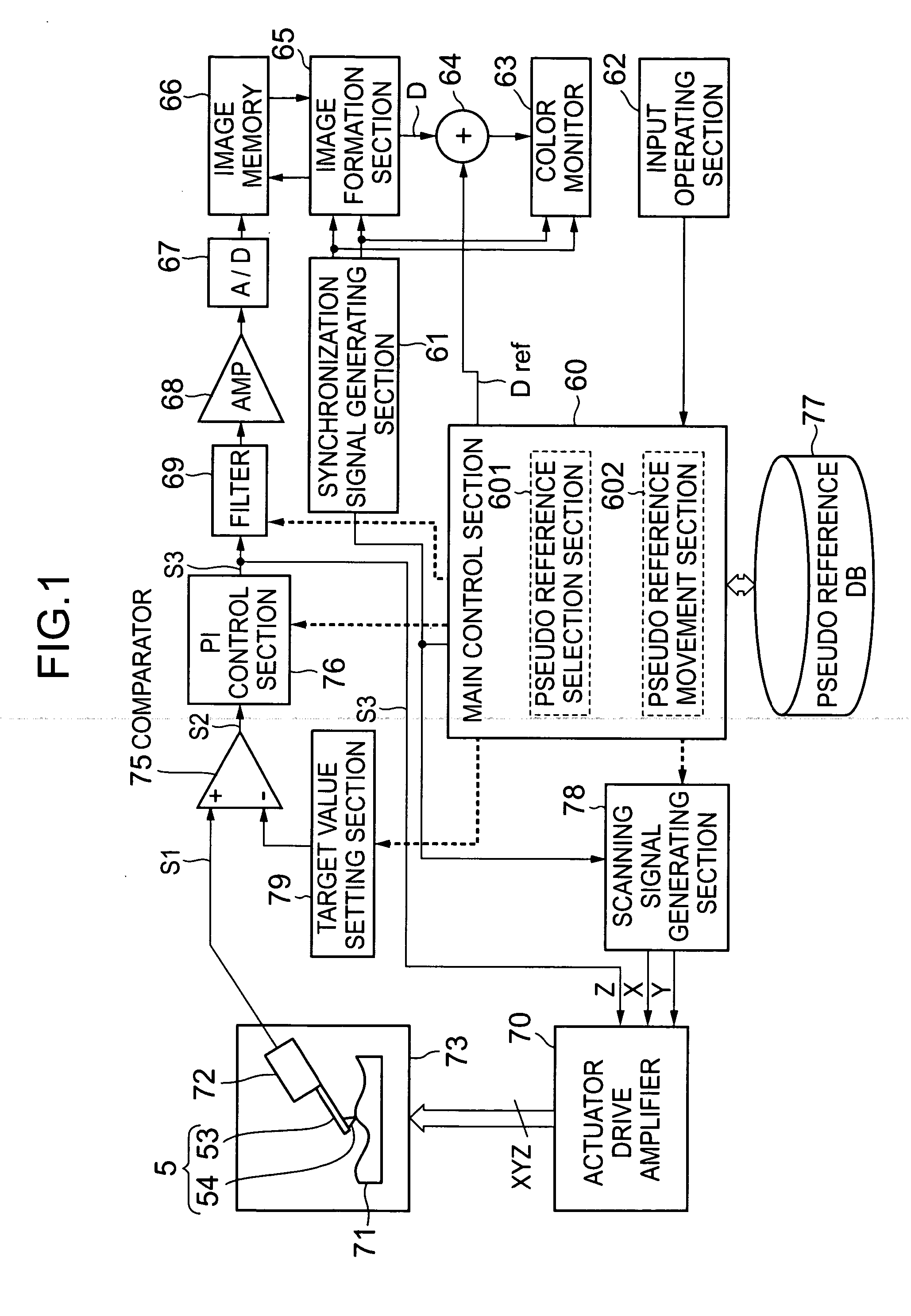
[0049]FIG. 14 is a block diagram of a scanning probe microscope adopting the present invention. The same reference numerals represent the same sections as previously described.
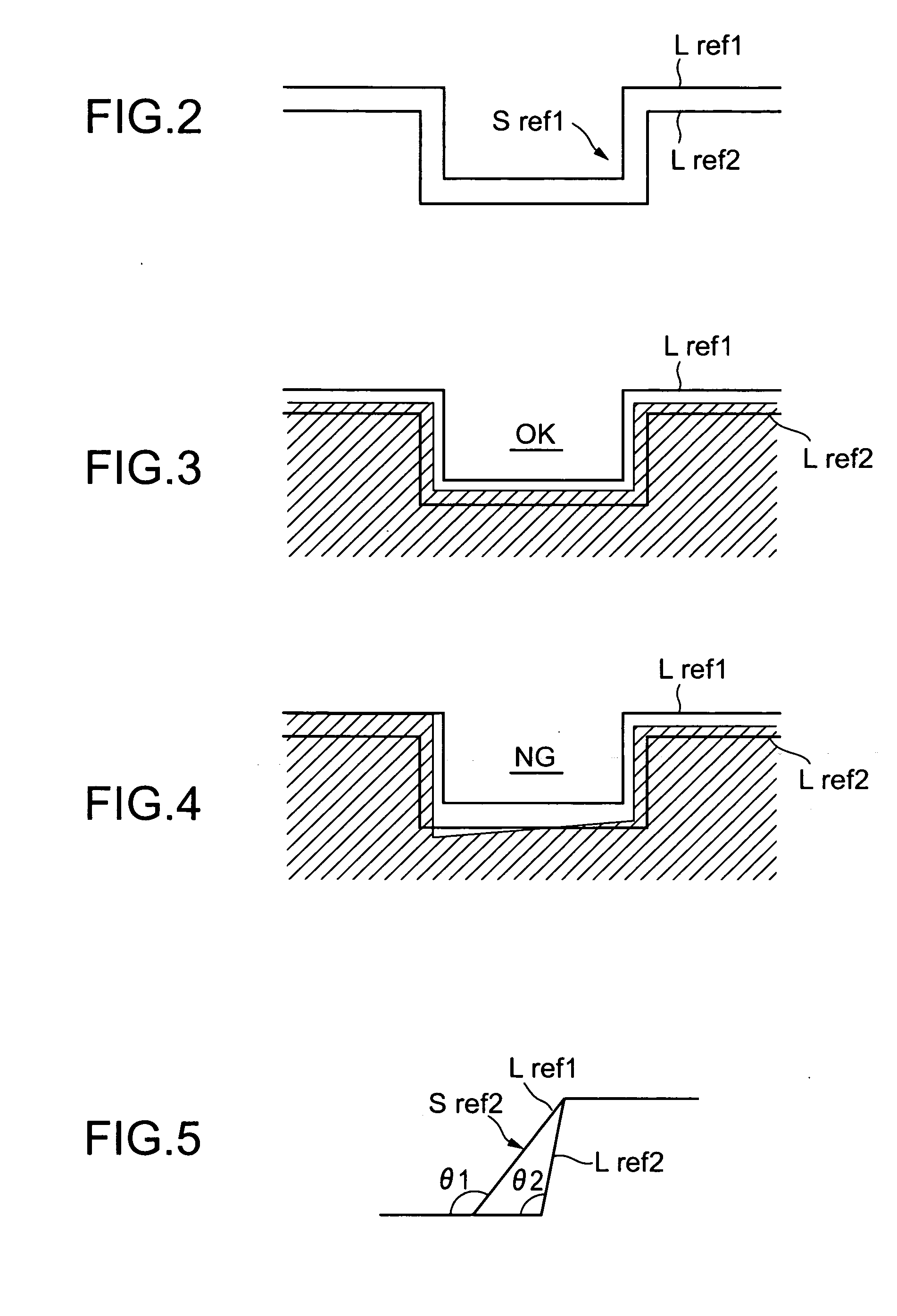
[0050] With this embodiment, an adding circuit 74 is added between the amplifier 68 and the A / D converter 67. A pseudo reference image Sref generated by the pseudo reference generating section 603 of the main control section 60 is superimposed on the output signal of the amplifier 68 and input to the A / D converter 67, and this superimposed signal is displayed on the color monitor 63.
[0051]FIG. 15 is a drawing showing the operation of the adding circuit 74. A signal at the time of not scanning, namely a noise component Sn, is input from the amplifier 68, and a reference rectangular wave Sc is input from the pseudo reference generating section 603 of the main control section 60. A peak value of the reference rectangular wave Sc is set to an upper limit value An of the noise level, and the frequency of the refer...
PUM
| Property | Measurement | Unit |
|---|---|---|
| scanning probe microscope | aaaaa | aaaaa |
| frequency | aaaaa | aaaaa |
| atomic force microscope | aaaaa | aaaaa |
Abstract
Description
Claims
Application Information