Semiconductor light-emitting device

a technology of semiconductor light and light-emitting device, which is applied in the direction of semiconductor/solid-state device manufacturing, semiconductor devices, electrical equipment, etc., can solve the problems of weaker light absorption, difficult to use resin molds to package semiconductor light, and inability to efficiently extract light. , to achieve the effect of easy recognition

Inactive Publication Date: 2014-06-03
SHARP KK
View PDF12 Cites 0 Cited by
  • Summary
  • Abstract
  • Description
  • Claims
  • Application Information

AI Technical Summary

Benefits of technology

[0014]In view of this, an object of the present invention is to provide a semiconductor light-emitting device which has a simple configuration and which makes it possible to easily and accurately confirm whether or not ultraviolet light is being emitted.
[0017]By visually observing the visible light, a user or a nearby person can thereby easily recognize whether or not ultraviolet light is being outputted from the semiconductor light-emitting device. Specifically, it is possible to easily confirm whether or not ultraviolet light is being emitted with a simple configuration.
[0026]According to the present invention, providing a UV-excited phosphor which is excited by ultraviolet light and which outputs visible light results in a structure in which the UV-excited phosphor is irradiated with some of the ultraviolet light outputted from the semiconductor light-emitting element; therefore, when the ultraviolet light is emitted from the semiconductor light-emitting element, visible light is outputted to the exterior by the UV-excited phosphor at the same time as the ultraviolet light. By visually confirming the visible light, a user or a nearby person can easily recognize whether or not ultraviolet light is being outputted from the semiconductor light-emitting device. When some of the ultraviolet light is absorbed by the translucent cover, the absorbed ultraviolet light can be transmitted as visible light to the outside of the translucent cover, and the light outputted from the semiconductor light-emitting element can therefore be effectively utilized.

Problems solved by technology

However, ultraviolet light is absorbed by the resin used in the resin mold and the light cannot be extracted efficiently.
The resin is deteriorated by the strong energy of ultraviolet light, causing a problem of stronger light absorption.
Therefore, it is difficult to use a resin mold to package a semiconductor light-emitting device that emits light in the ultraviolet region.
Light in the regions ultraviolet to deep ultraviolet have much energy and can adversely affect the human body in the eyes, skin, and the like.
When it is not possible to assess what range is being irradiated by the ultraviolet light (*1), problems with safety occur also when the device is actually used.
Therefore, the light-emitting state of a semiconductor light-emitting device that emits light in the regions ultraviolet to deep ultraviolet can be confirmed utilizing a detector capable of detecting ultraviolet light, but it is troublesome to use a detector for this confirmation.
When the device is utilized in common sanitary appliances or medical appliances, the common user is not likely to possess a detector and it is not easy to confirm the output of ultraviolet light.
Because of this, the ultraviolet-light-emitting device disclosed in Japanese Laid-open Patent Application No. 2009-177098 has numerous configurationally members, and it is difficult to reduce this device in size and cost.
There are also cases in which the ultraviolet-light-emitting device is disposed inside another device, in which case it is sometimes difficult or even impossible to ascertain the starting light LED chip for monitoring, and it is sometimes difficult to accurately confirm whether or not the ultraviolet-light-emitting device has activated.

Method used


Image

  • Semiconductor light-emitting device
  • Semiconductor light-emitting device
  • Semiconductor light-emitting device

Examples


first embodiment

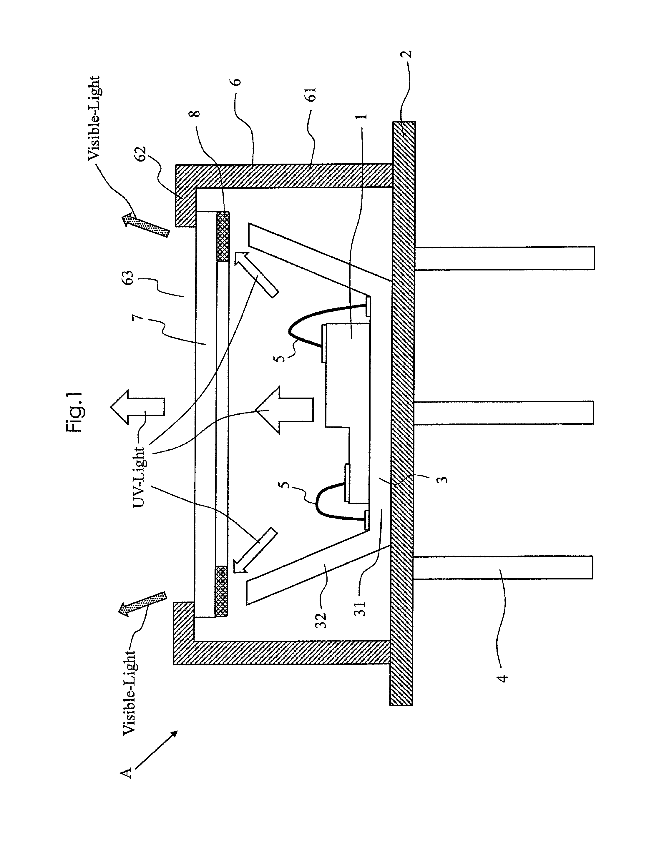
[0040]As shown in FIG. 1, the semiconductor light-emitting device A according to the present invention is packaged. The semiconductor light-emitting device A has a configuration in which a nitride semiconductor light-emitting element 1 (may hereinafter be called simply as an LED element 1) for outputting ultraviolet light is disposed in a metal package referred to as a CAN package.

[0041]The semiconductor light-emitting device A comprises the LED element 1, a circular plate-shaped holding base (stem) 2 for holding the LED element 1, a reflective cup 3 which is mounted on the holding base 2 and which reflects the light outputted by the LED element 1 back upward, external pins 4 which protrude from the holding base 2 and supply power to the semiconductor light-emitting device A, wires 5 for supplying the LED element 1 with the power supplied via the external pins 4, and a metal cap part 6 called a CAN which encloses the LED element 1. The semiconductor light-emitting device A also comp...

second embodiment

[0085]Another example of the semiconductor light-emitting device according to the present invention will be described referring to the drawings. FIG. 8 is a drawing of another example of a semiconductor light-emitting device according to the present invention. As shown in FIG. 8, in the semiconductor light-emitting device B, a UV-excited phosphor 81 is disposed on the side wall part 32 of the reflective cup 3 disposed inside the cap part 6, but the configuration is otherwise the same as the semiconductor light-emitting device A. Portions of the same substance are not described in detail. The nitride semiconductor light-emitting element 1 also uses the same configuration as that of the semiconductor light-emitting device A.

[0086]Even in a configuration comprising the UV-excited phosphor 81 on part of the side wall part 32 of the reflective cup 3, visible light is outputted by the UV-excited phosphor 81, and the light-emitting state of the semiconductor light-emitting device B can be ...

third embodiment

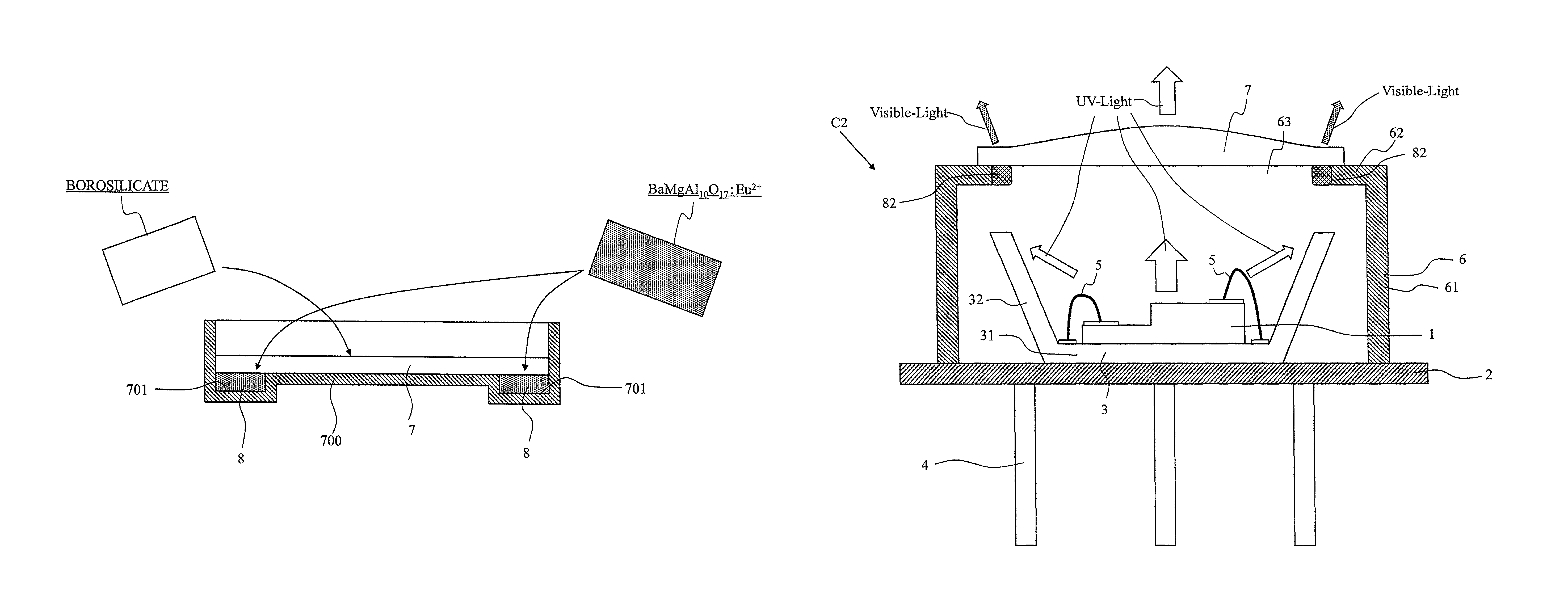
[0091]Yet another example of the semiconductor light-emitting device according to the present invention will be described with reference to the drawings. FIG. 9 is a drawing of yet another example of the semiconductor light-emitting device according to the present invention. Aside from the translucent cover 7 being disposed on the outside of the cap part 6, the semiconductor light-emitting device C shown in FIG. 9 has the same configuration as the semiconductor light-emitting device A shown in FIG. 1, and components that are essentially the same are not described in detail. A nitride semiconductor light-emitting element 1 having the same configuration as that of the semiconductor light-emitting device A is also used.

[0092]Due to the translucent cover 7 being disposed on the outside of the cap part 6, irradiation of the connecting part between the translucent cover 7 and the cap part 6 with ultraviolet light can be suppressed by the blocking of light from the LED element 1 by the cap...


PUM


Abstract

A semiconductor light-emitting device (A) having a simple configuration whereby it is possible to easily and accurately confirm whether or not ultraviolet light is being emitted, the semiconductor light-emitting device comprising: a semiconductor light-emitting element (1) for emitting ultraviolet light in an ultraviolet or deep ultraviolet region; a cap part (6) having a through-hole (63) in the top part through which ultraviolet light passes and encircling the semiconductor light-emitting element (1); a translucent cover (7) for transmitting ultraviolet light, the translucent cover being disposed so as to hermetically close up the through-hole (63); and a UV-excited phosphor (8) which is excited by ultraviolet light and which emits visible light, the UV-excited phosphor being disposed inside the cap part (6).

Description

[0001]This application is based on Japanese Patent Application No. 2011-179583 filed on Aug. 19, 2011.BACKGROUND OF THE INVENTION[0002]1. Field of the Invention[0003]The present invention relates to a semiconductor light-emitting device for irradiating with ultraviolet rays.[0004]2. Description of Related Art[0005]Nitride semiconductors, typified by GaN, AlN, InN, and mixed crystals thereof, are direct-transition semiconductor materials. Nitride semiconductors have the characteristic of having greater band gap energy than AlGaInAs-based semiconductors or AlGaInP-based semiconductors. Therefore, these nitride semiconductors are being focused on as materials constituting semiconductor laser elements for emitting light in the ultraviolet region, LED elements for emitting light in the ultraviolet region or the deep ultraviolet region (a wavelength range of approximately 320 nm to approximately 200 nm), and other semiconductor light-emitting elements.[0006]Light in the ultraviolet region...

Claims


Application Information

Patent Timeline
Patent Type & Authority Patents(United States)
IPC IPC(8): H01L33/00H01L21/00
CPCH01L33/507H01L33/483H01L2224/48091H01L2224/49107H01L2924/00014
Inventor OHTA, MASATAKAKAMIKAWA, TAKESHI
Owner SHARP KK
Why Eureka
Try Eureka