

structure and method of manufacturing a finFet device having stacked fins
- Summary
- Abstract
- Description
- Claims
- Application Information
AI Technical Summary
Benefits of technology
Problems solved by technology
Method used
Image

Examples
Embodiment Construction
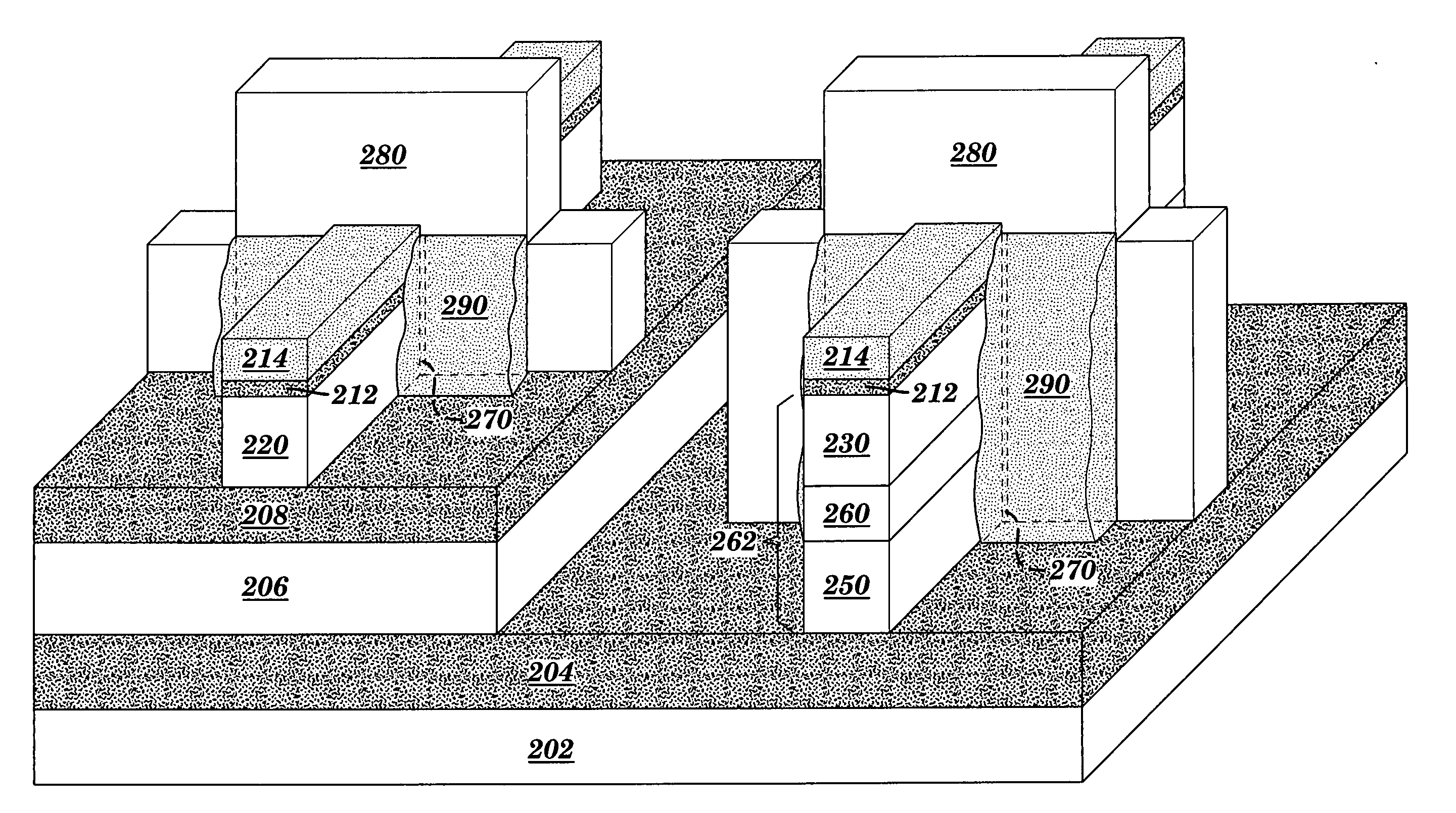
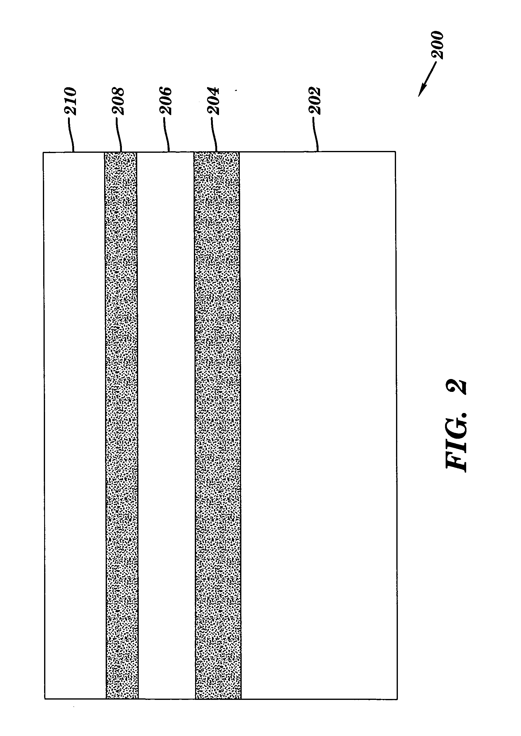
[0023] The present invention thus provides a device structure and method of forming fin Field Effect Transistors (finFETs) that overcome many of the disadvantages of the prior art. Specifically, the device structure and method provide the ability to form finFET devices with improved circuit density while accounting for mobility differences by forming a finFET device with a single fin n-finFET and a stacked double fin p-finFET. Additionally, the device structure and method provide the ability to form finFET devices that utilize various crystal planes in order to optimize mobility and / or reduce mobility in specific devices. Finally, the device structure and method provide improved fin height control by forming finFETs from multiple silicon layers having buried oxide layers in between the silicon layers, the buried oxide layers acting as a silicon etch stop.
[0024] The invention will next be illustrated with reference to the figures in which the same numbers indicate the same elements ...
PUM
 Abstract
Description
Claims
Application Information