High density laminated substrate structure and manufacture method thereof

Inactive Publication Date: 2005-12-20
VIA TECH INC
View PDF26 Cites 55 Cited by
  • Summary
  • Abstract
  • Description
  • Claims
  • Application Information

AI Technical Summary

Benefits of technology

[0011]Therefore, the object of the present invention is to provide a laminated substrate structure, in which a landless design

Problems solved by technology

When the laminated substrate is made by using the conventional lamination process, the via forming, plating through hole and the isolation material hole plugging operations must be performed on the isolation layer, and the process is rather sophisticated and time consuming.
Moreover, the process difficulty and unit cost significantly increase accordingly when the isolation layer via dimension approaches 100 micrometers or below.
Therefore, there is a mass production technology bottleneck problem when the plating through hole is less than 100 micrometers.
In the substrate formed by the build up process, each dielectric layer and circuit layer has to be formed sequentially, so that

Method used


Image

  • High density laminated substrate structure and manufacture method thereof
  • High density laminated substrate structure and manufacture method thereof
  • High density laminated substrate structure and manufacture method thereof

Examples


first embodiment

[0030]The First Embodiment

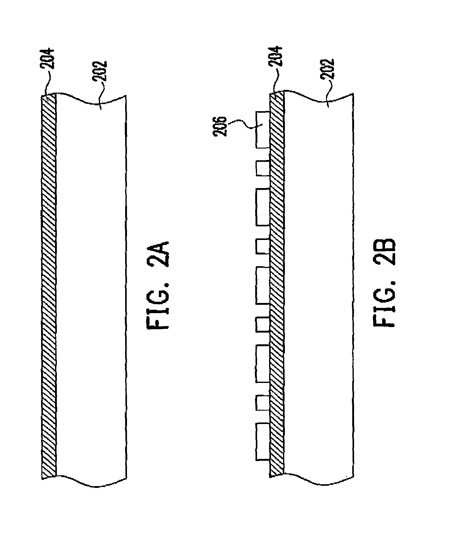
[0031]FIGS. 2A–2D schematically show a sectional sketch views of the manufacture process of the circuit parts that have a patterned circuit in the laminated substrate of the first embodiment according to the present invention. The patterned circuit in the laminated substrate of the present invention is formed by using a method such as metal etching, pattern plating, semi-additive, or full-additive. Metal etching is used in the present embodiment for description. Referring to FIG. 2A first, a supporter 202 is provided, and a conductive layer 204 is subsequently formed on the supporter 202. The conductive layer 204 is made of material such as copper, and the conductive layer 204 is formed on the supporter 202 by using a method such as sputtering, lamination adherence or deposition.

[0032]Referring to both FIG. 2B and FIG. 2C simultaneously, a patterned photoresist 206 is subsequently formed on the conductive layer 204, the patterned photoresist 206 is used to ...

second embodiment

[0040]The Second Embodiment

[0041]The present embodiment is the same as the first embodiment in forming the dielectric layer having the via studs and the via opening layer. The difference between the present embodiment and the first embodiment is in the manufacture method of the dielectric layer having the patterned circuit.

[0042]FIGS. 6A–6D schematically shows sectional sketch views of the manufacture process of the dielectric layer that has a patterned circuit in the laminated substrate of the second embodiment according to the present invention. Referring to FIG. 6A first, a supporter 602 is provided, and a conductive layer 604 is subsequently formed on the supporter 602. The conductive layer 604 is made of material such as copper, and the conductive layer 604 is formed on the supporter 602 by using a method such as sputtering, lamination adherence or deposition.

[0043]Then, referring to both FIG. 6B and FIG. 6C simultaneously, a patterned photoresist 606 is subsequently formed on ...


PUM

PropertyMeasurementUnit
Dielectric polarization enthalpyaaaaaaaaaa
Densityaaaaaaaaaa

Abstract

A laminated substrate structure composed of a plurality of dielectric layers and a plurality of circuit layers stacked with each other. Each of the dielectric layers has a plurality of via studs, and the circuit layers are electrically coupled with each other through the via studs. The laminated substrate structure of the present invention is characterized by adopting the embedded structure landless design that provides high reliability and better adherence. The present invention also provides a laminated substrate manufacture method. The dielectric layers having the patterned circuit and the dielectric layers having the via holes are formed first, and after the dielectric layers having the patterned circuit and the dielectric layers having the via holes are formed, they are aligned and laminated synchronously to complete the manufacture of the laminated substrate.

Description

CROSS REFERENCE TO RELATED APPLICATIONS[0001]This application claims the priority benefit of Taiwan application serial no. 91111329, filed May 28, 2002.BACKGROUND OF INVENTION[0002]1. Field of Invention[0003]The present invention generally relates to a laminated substrate structure and the manufacture method thereof, and more particularly, to a package substrate or Printed Circuit Board (PCB) structure and the manufacture method thereof.[0004]2. Description of Related Art[0005]In line with fast growth and the high demand for electronic technology, the development of electronic products tends towards miniaturization and high density integration. In the packaging field, the development of the Ball Grid Array (BGA) and Chip Scale Package (CSP) is targeted at the market requirements for miniaturization and high-density integration. For the Printed Circuit Board (PCB), in order to minimize the circuit area used, the technology of the multi-layered structure is applied. However, the subst...

Claims


Application Information

Patent Timeline
IPC IPC(8): H05K3/20H05K3/28H05K3/46
CPCH05K3/4617H05K3/20H05K3/281H05K2201/09545Y10T428/24917H05K2203/063H05K2203/0733Y10T428/24851Y10T428/24331H05K2201/10378
Inventor HO, KWUN-YAOKUNG, CHEN-YUEH
Owner VIA TECH INC
Why Eureka
Try Eureka