Wide bandgap field effect transistors with source connected field plates

a field effect transistor and source connected technology, applied in the field of field effect transistors utilizing field plates, can solve the problems of significant field plate to drain capacitance, limiting the performance of these devices, and affecting the performance of the device,

Active Publication Date: 2005-11-17
CREE INC
View PDF104 Cites 49 Cited by
  • Summary
  • Abstract
  • Description
  • Claims
  • Application Information

AI Technical Summary

Benefits of technology

[0008] The present invention provides improved field effect transistors having a field plate connected to the source electrode. One embodiment of a field effect transistor according to the present invention comprises a metal semiconductor field effect transistor (MESFET) having a buffer layer on a substrate and a channel layer on the buffer layer with the buffer layer sandwiched between the channel layer and substrate. A source electrode is included in electrical contact with said plurality of the ch

Problems solved by technology

Electron trapping and the resulting difference between DC and RF characteristics have been a limiting factor in the performance of these devices.
However, due to the high electric fields existing in these structures, charge trapping is still an issue.
This can

Method used


Image

  • Wide bandgap field effect transistors with source connected field plates
  • Wide bandgap field effect transistors with source connected field plates
  • Wide bandgap field effect transistors with source connected field plates

Examples


Embodiment Construction

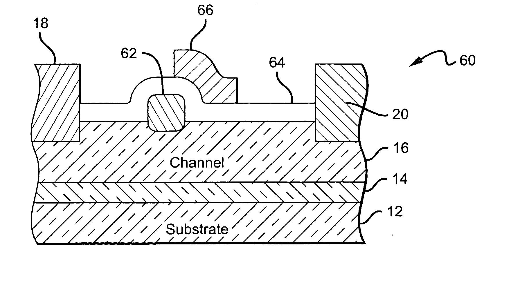
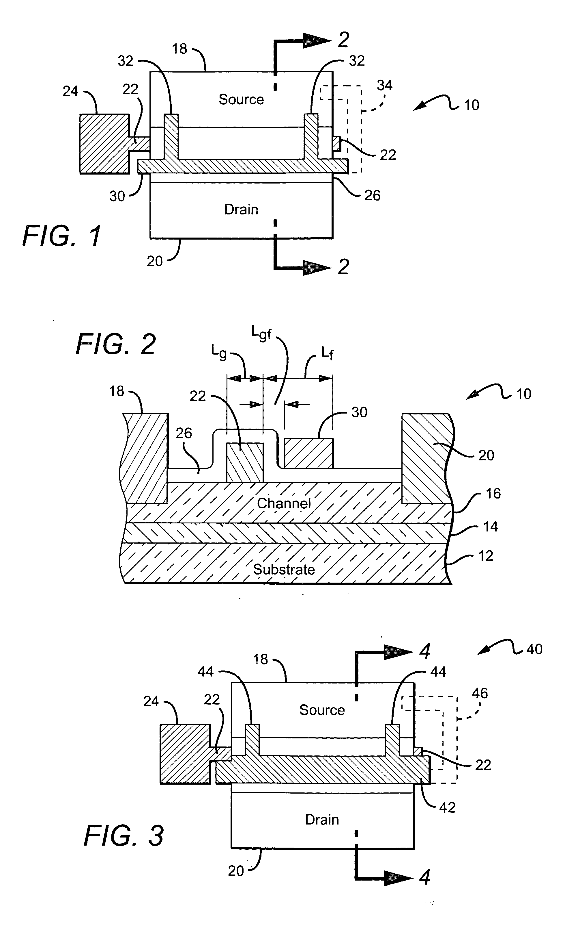
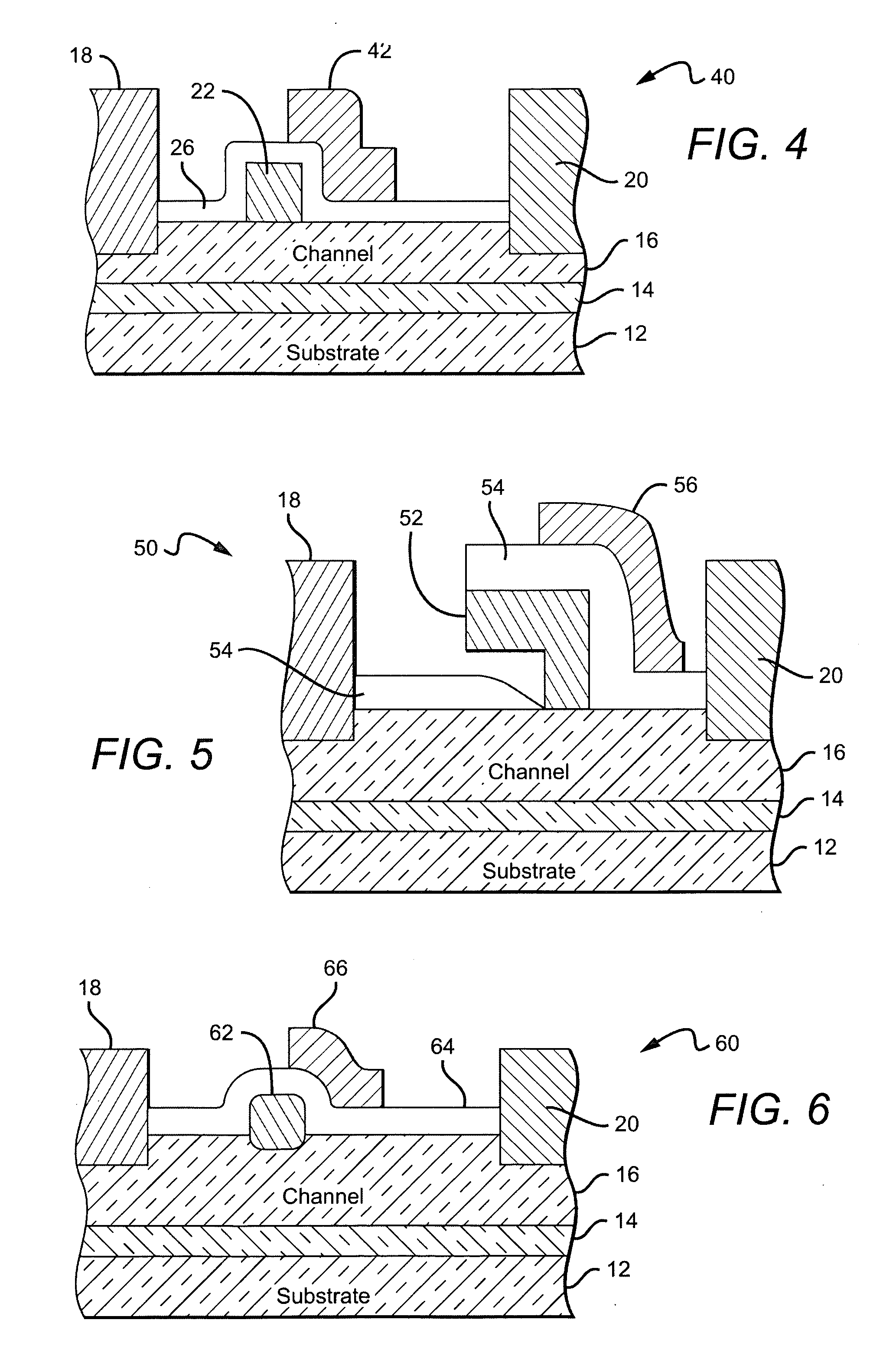
[0018] The field plate arrangements according to the present invention can be used with many different transistor structures. Wide bandgap transistor structures generally include an active region, with metal source and drain electrodes formed in electrical contact with the active region, and a gate electrode formed between the source and drain electrodes for modulating electric fields within the active region. A spacer layer is formed above the active region. The spacer layer can comprise a dielectric layer, or a combination of multiple dielectric layers. A conductive field plate is formed on the spacer layer and extends a distance Lf from the edge of the gate electrode toward the drain electrode.

[0019] The field plate can be electrically connected to the source electrode. This field plate arrangement can reduce the peak electric field in the device, resulting in increased breakdown voltage and reduced trapping. The reduction of the electric field can also yield other benefits such...


PUM


Abstract

A field effect transistor comprising a buffer and channel layer formed successively on a substrate. A source electrode, drain electrode, and gate are all formed in electrical contact with the channel layer, with the gate between the source and drain electrodes. A spacer layer is formed on at least a portion of a surface of the channel layer between the gate and drain electrode and a field plate is formed on the spacer layer isolated from the gate and channel layer. The spacer layer is electrically connected by at least one conductive path to the source electrode, wherein the field plate reduces the peak operating electric field in the MESFET.

Description

[0001] This application claims the benefit of provisional application Ser. No. 60 / 571,342 to Wu et al., which was filed on May 13, 2004.BACKGROUND OF THE INVENTION [0002] 1. Field of the Invention [0003] The present invention relates to transistors and particularly to field effect transistors utilizing field plates. [0004] 2. Description of the Related Art [0005] Improvements in the manufacturing of AlGaN / GaN semiconductor materials have helped advance the development of AlGaN / GaN transistors, such as high electron mobility transistors (HEMTs) for high frequency, high temperature and high power applications. AlGaN / GaN has large bandgaps, high peak and saturation electron velocity values [B. Gelmont, K. Kim and M. Shur, Monte Carlo Simulation of Electron Transport in Gallium Nitride, J. Appl. Phys. 74, (1993), pp. 1818-1821]. [0006] Electron trapping and the resulting difference between DC and RF characteristics have been a limiting factor in the performance of these devices. Silicon...

Claims


Application Information

Patent Timeline
IPC IPC(8): H01L29/06H01L29/20H01L29/40H01L29/41H01L29/417H01L29/812H01L31/0328
CPCH01L29/2003H01L29/812H01L29/41725H01L29/402H01L29/42316H01L29/1608H01L21/18
Inventor WU, YIFENGPARIKH, PRIMITMISHRA, UMESHMOORE, MARCIA
Owner CREE INC
Why Eureka
Try Eureka