Photoelectric converting film stack type solid-state image pickup device

a technology of photoelectric and solid-state image, which is applied in the direction of television system, television system scanning details, radioation control devices, etc., can solve the problems of reducing resolution, false color, and inability to increase the area of light receiving portions, so as to achieve the effect of enhancing the resolution in the row direction

Inactive Publication Date: 2005-12-01
FUJIFILM CORP
View PDF4 Cites 18 Cited by
  • Summary
  • Abstract
  • Description
  • Claims
  • Application Information

AI Technical Summary

Benefits of technology

[0030] According to the configuration, even when the dimension of each pixel electrode film in the row direction is larger than that in the column direction, the resolution in the row direction can be enhanced.

Problems solved by technology

In the related-art solid-state image pickup device, therefore, many light receiving portions and signal read circuits must be formed on the same surface of a semiconductor substrate, thereby producing a problem in that the area for the light receiving portions cannot be increased.
This causes a false color, and reduces the resolution.
Furthermore, blue light and green light incident on a light receiving portion where a red color filter is formed do not contribute to photoelectric conversion, but are absorbed as heat into the color filter, thereby producing another problem in that the light use efficiency is poor and the sensitivity is low.
As described above, the related-art solid-state image pickup device has various problems.
Consequently, a CCD device and a CMOS device are hardly expected to configure an image sensor which can solve the above-discussed problems, and which is superior in image quality and sensitivity than the related-art one.
In the vertical transfer paths 11r, 11g, 11b, therefore, the widths of the vertical transfer paths below the first-phase transfer electrode Φv1 are narrowed, and there arises a trouble that the transfer efficiency is reduced by the narrow-channel effect.
As a result, the pixel pitch in the row (horizontal) direction cannot be reduced, and a photoelectric converting film stack type solid-state image pickup device of a high resolution cannot be realized.
Therefore, the configuration of FIG. 6 has a problem in that the maximum quantity of transferred charges is largely restricted by the first-phase transfer electrode Φv1 and the saturation power is reduced.
It is difficult to realize a photoelectric converting film stack type solid-state image pickup device having a wide dynamic range.

Method used


Image

  • Photoelectric converting film stack type solid-state image pickup device
  • Photoelectric converting film stack type solid-state image pickup device
  • Photoelectric converting film stack type solid-state image pickup device

Examples


first embodiment

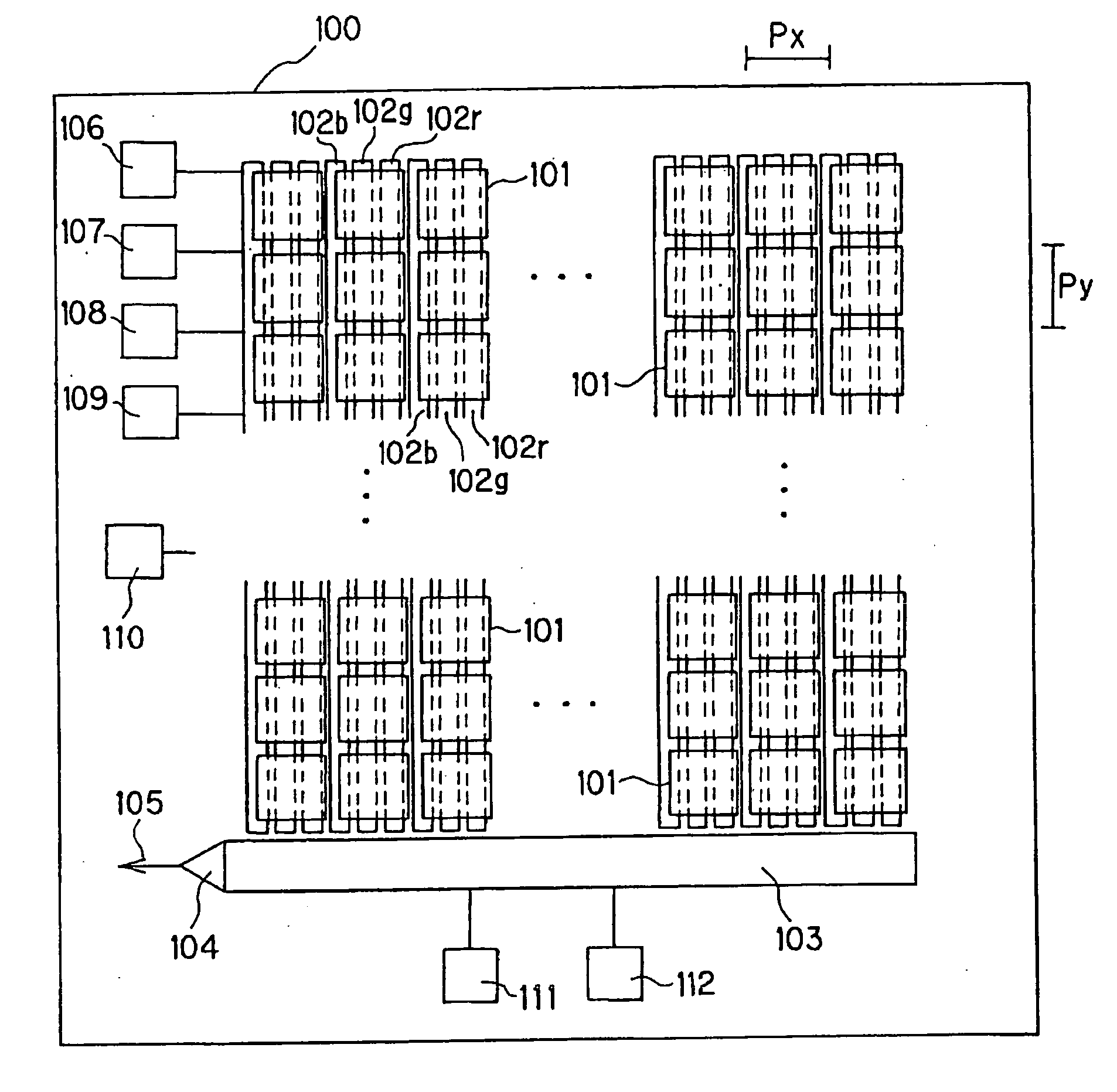
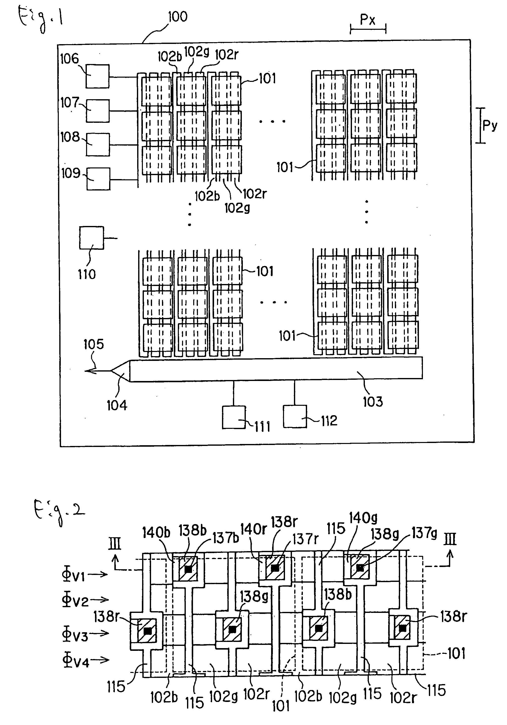
[0038]FIG. 1 is a surface diagram of a photoelectric converting film stack type solid-state image pickup device of a first embodiment of the invention. In the photoelectric converting film stack type solid-state image pickup device 100, many light receiving portions (pixels) 101 are arranged in, in this example, a lattice manner. The light receiving portions 101 are arranged at a pixel pitch Px in the horizontal direction (row direction), and at a pixel pitch Py in the vertical direction (column direction).

[0039] On the surface of a semiconductor substrate which is disposed below the light receiving portions 101 of the photoelectric converting film stack type solid-state image pickup device 100, three vertical transfer paths (column CCD registers) 102b, 102g, 102r (the suffixes b, g, r correspond to blue (B), green (G), and red (R), respectively, and the same shall apply hereinafter) are formed in correspondence with the columns of the light receiving portions 101 which are arrange...

second embodiment

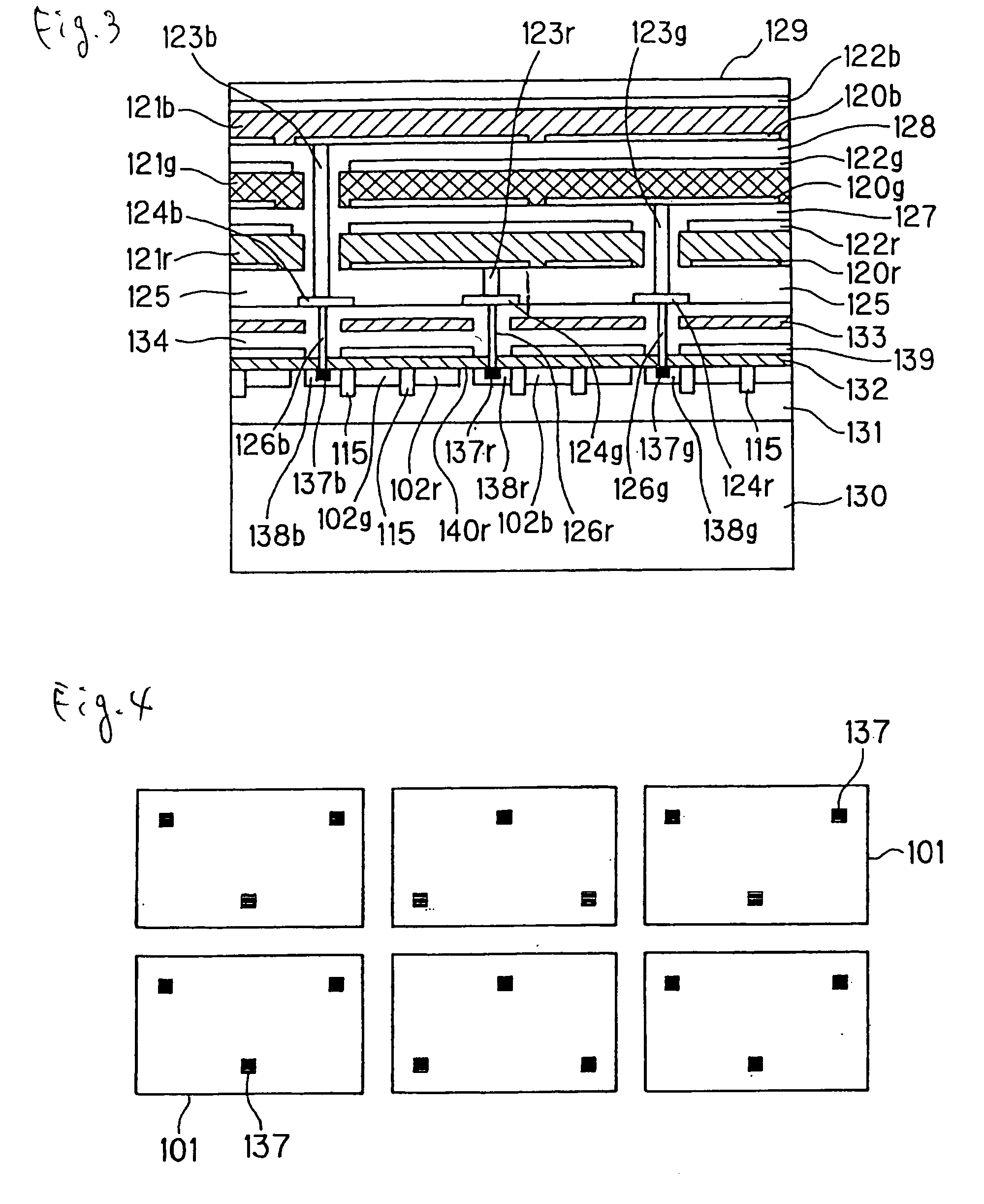
[0060]FIG. 4 is a surface diagram of six pixels of a photoelectric converting film stack type solid-state image pickup device of a second embodiment of the invention.

[0061] In the photoelectric converting film stack type solid-state image pickup device of the first embodiment shown in FIG. 1, the pixel pitch Px in the horizontal direction is equal to the pixel pitch Py in the vertical direction. Furthermore, four transfer electrodes and three vertical transfer paths are disposed in one pixel. For example, the charge accumulating portion 138g adjacent to the charge accumulating portion 138b shown in FIG. 2 is therefore placed with being shifted with respect to the portion 138b by one-third of the pixel pitch or Px / 3 in the horizontal direction, and by one-half of the pixel pitch or Py / 2 in the vertical direction.

[0062] In the design of the signal read portions for the vertical transfer paths (in the embodiment, the design of the charge accumulating portions because the signal read ...

third embodiment

[0064]FIG. 5 is a surface diagram of main portions of a photoelectric converting film stack type solid-state image pickup device of a third embodiment of the invention.

[0065] In the first and second embodiments, the pixel electrode films 120r, 120g, 120b of each pixel 101 are aligned with each other in the direction of incident light. By contrast, the embodiment has the configuration of FIG. 4, or the degree of integration of the CCD signal read portions is largest, and is different in that each of the pixel electrode films 120r, 120g, 120b is shifted by Px / 3 in the horizontal direction. According to the configuration, although colors are different, image data which are shifted by Px / 3 can be obtained. When the interpolating calculation of image data in the horizontal direction is conducted, the resolution can be enhanced.

[0066] In FIG. 5, the pixel electrode films 120r, 120g, 120b are shown with being slightly shifted also in the vertical direction. This is conducted in order to ...


PUM


Abstract

A solid-state image pickup device comprises: a semiconductor substrate; at least one photoelectric converting film that generates signal charges corresponding to an amount of incident light; at least one set of pixel electrode films arranged in row and column directions and attached to said at least one photoelectric converting film; vertical transfer paths in the semiconductor substrate, extended in the column direction; and charge accumulating portions in the surface portion of the semiconductor substrate that accumulate signal charges from the pixel electrode films, wherein the charge accumulating portions comprise a plurality of sets, each comprising a subset of the charge accumulating portions arranged in the column direction, and wherein the subset reads out the accumulated signal charges to the corresponding one of the vertical transfer paths, and wherein the two adjacent subsets of the charge accumulating portions are shifted to each other in a direction along the vertical transfer paths.

Description

BACKGROUND OF THE INVENTION [0001] 1. Field of the Invention [0002] The present invention relates to a photoelectric converting film stack type solid-state image pickup device in which a photoelectric converting film that generates charges corresponding to the amount of received light is stacked on a semiconductor substrate, and more particularly to a photoelectric converting film stack type solid-state image pickup device in which a signal charge generated in a photoelectric converting film is transferred through a charge transfer path on a semiconductor substrate to be read out to the outside. [0003] 2. Description of the Related Art [0004] In a CCD solid-state image pickup device or a CMOS solid-state image pickup device which is mounted on a digital camera, a large number of photoelectric converting elements (photodiodes) serving as light receiving portions, and signal read circuits which read out photoelectric conversion signals obtained in the photoelectric converting elements...

Claims


Application Information

Patent Timeline
Patent Type & Authority Applications(United States)
IPC IPC(8): H01L27/146H01L31/10H04N5/335H04N5/355H04N5/369
CPCH01L27/14603H01L27/14609H04N2209/047H01L27/14647H01L27/14687H01L27/14636
Inventor SUZUKI, NOBUOMASUKANE, KAZUYUKI
Owner FUJIFILM CORP
Why Eureka
Try Eureka