

Method and apparatus of distributed plasma processing system for conformal ion stimulated nanoscale deposition process
a technology of conformal ion and nanoscale deposition, applied in the field of conformal thin film deposition methods and apparatuses, can solve the problems of affecting the overall yield, affecting the coverage of the step, and the requirement of deposition becoming more critical, and achieves the effect of improving the coverage characteristics and high aspect ratio features
- Summary
- Abstract
- Description
- Claims
- Application Information
AI Technical Summary
Benefits of technology
Problems solved by technology
Method used
Image

Examples
Embodiment Construction
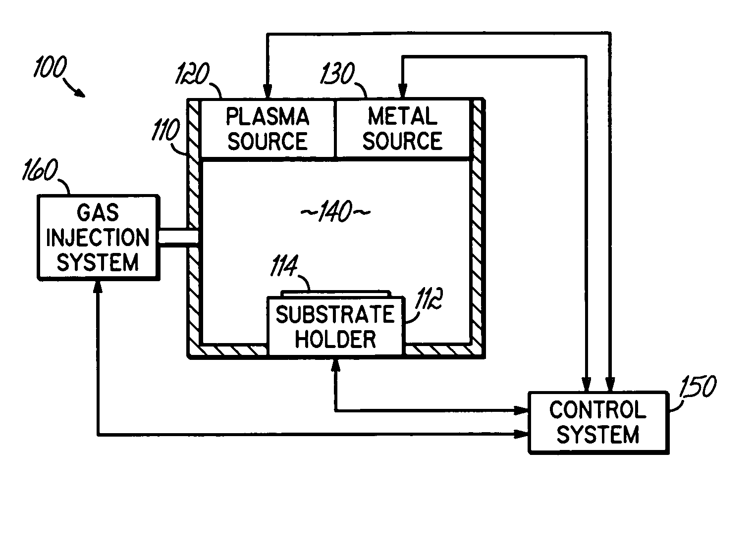
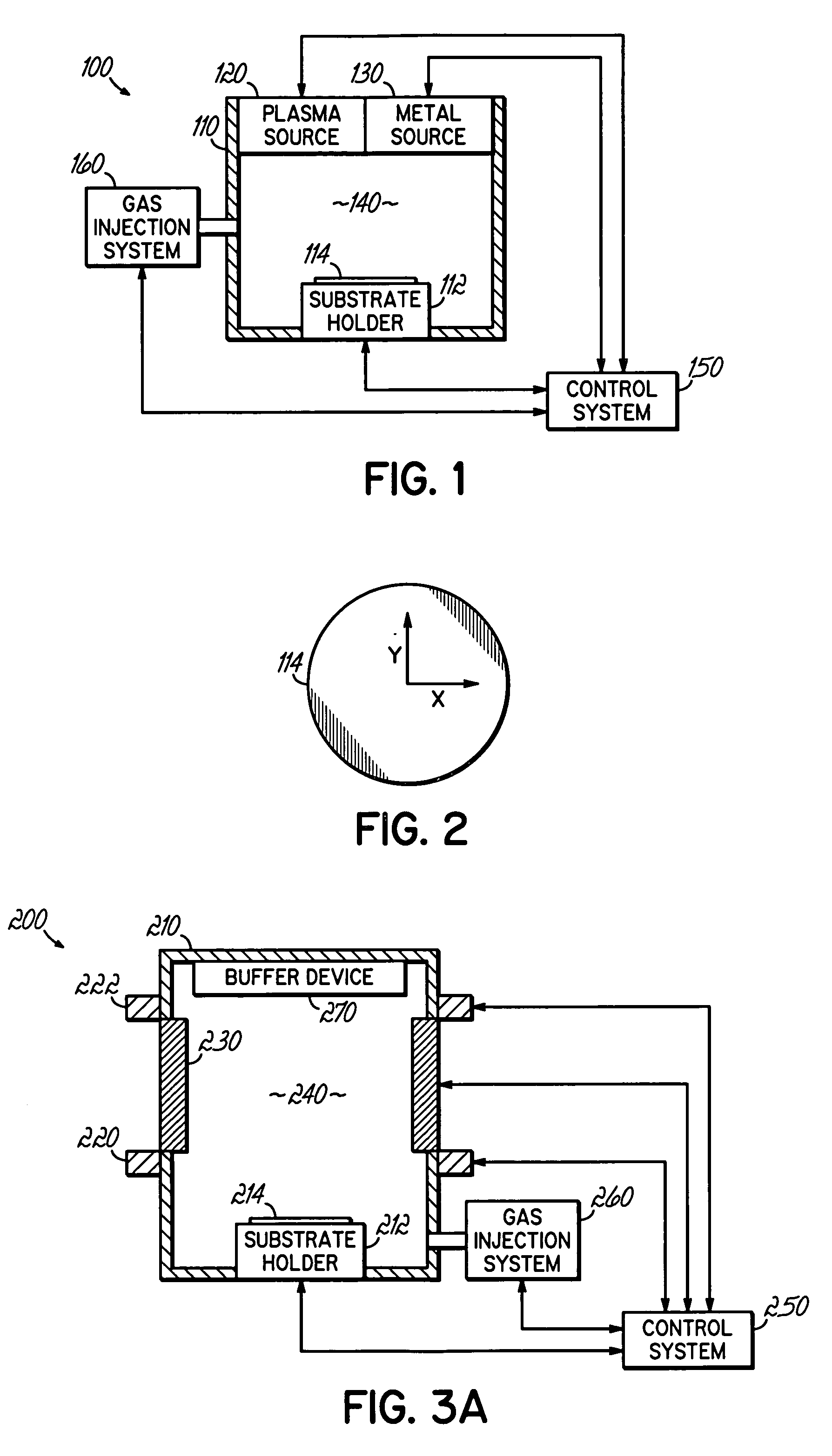
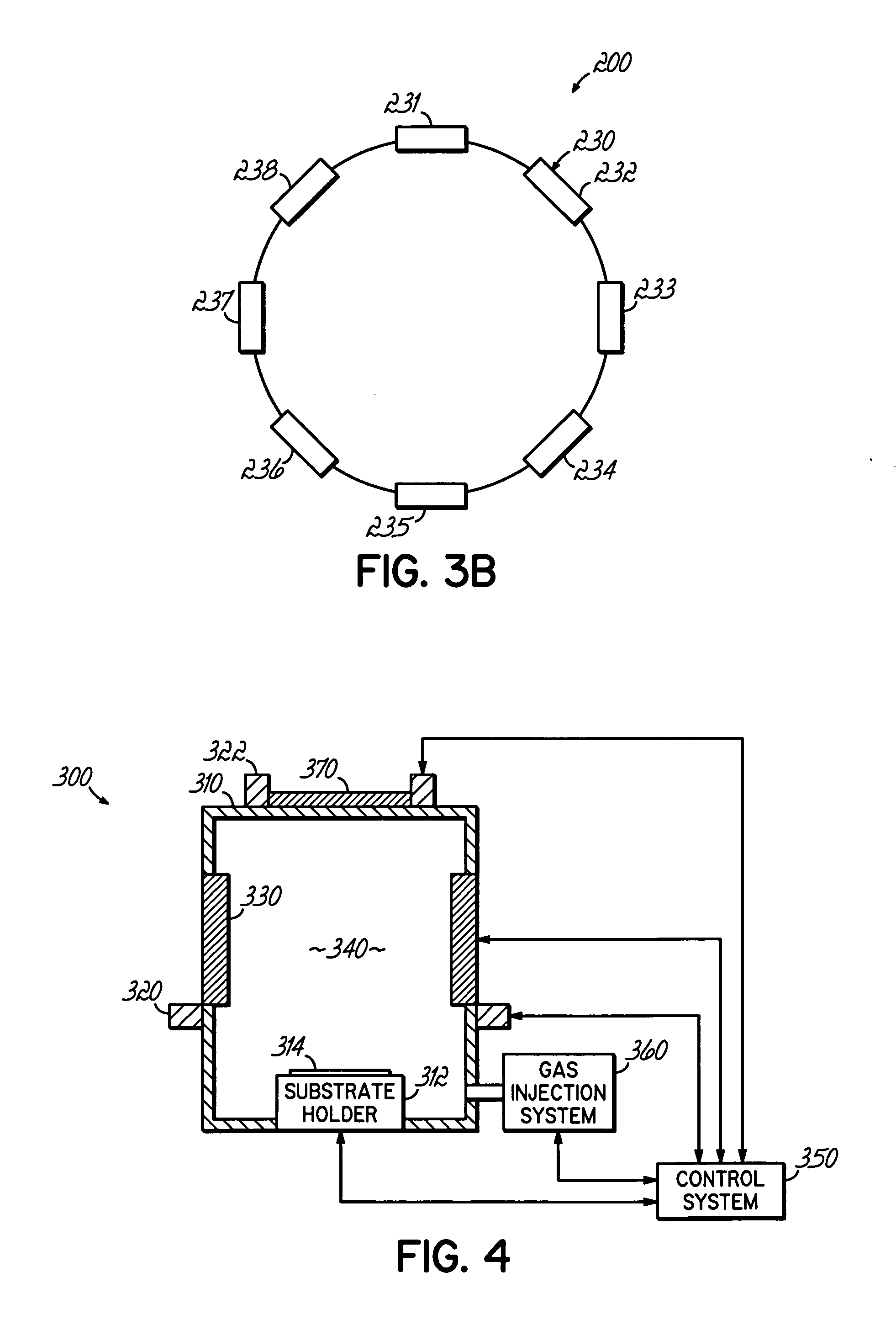
[0037] In the following description, in order to facilitate a thorough understanding of the invention and for purposes of explanation and not limitation, specific details are set forth, such as a particular geometry of the deposition system and various shapes of the plasma source and the distributed metal source. However, it should be understood that the invention may be practiced in other embodiments that depart from these specific details.
[0038] Nonetheless, it should be appreciated that, contained within the description are features which, notwithstanding the inventive nature of the general concepts being explained, are of an inventive nature.
[0039] For example, inventive aspects of the present disclosure include providing a deposition system and method for forming a thin film in a high aspect ratio feature on a substrate wherein a plasma source is coupled to a process chamber and configured to form a high density plasma of greater than 1012 e / cm3 (electrons per cubic centimete...
PUM
| Property | Measurement | Unit |
|---|---|---|
| pressure | aaaaa | aaaaa |
| aspect ratio | aaaaa | aaaaa |
| thickness | aaaaa | aaaaa |
Abstract
Description
Claims
Application Information