Method of forming pattern for semiconductor device

Active Publication Date: 2005-12-01
SAMSUNG ELECTRONICS CO LTD
View PDF4 Cites 2 Cited by
  • Summary
  • Abstract
  • Description
  • Claims
  • Application Information

AI Technical Summary

Problems solved by technology

Unfortunately, however, a thin photoresist pattern is generally susceptible to being etched during etching of the semiconductor substrate, thereby distorting the photoresist pattern.
In addition, in the event that the semiconductor substrate contains silicon, silicon byproducts are often produced on the photoresist

Method used


Image

  • Method of forming pattern for semiconductor device
  • Method of forming pattern for semiconductor device
  • Method of forming pattern for semiconductor device

Examples


Example

[0022] Exemplary embodiments of the invention are described below with reference to the corresponding drawings. These embodiments are presented as teaching examples. The actual scope of the invention is defined by the claims that follow. In the description it will be understood that where a layer is described as being “on” or “onto” another layer, the layers may be directly in contact with each other, or intervening layers may also be present.

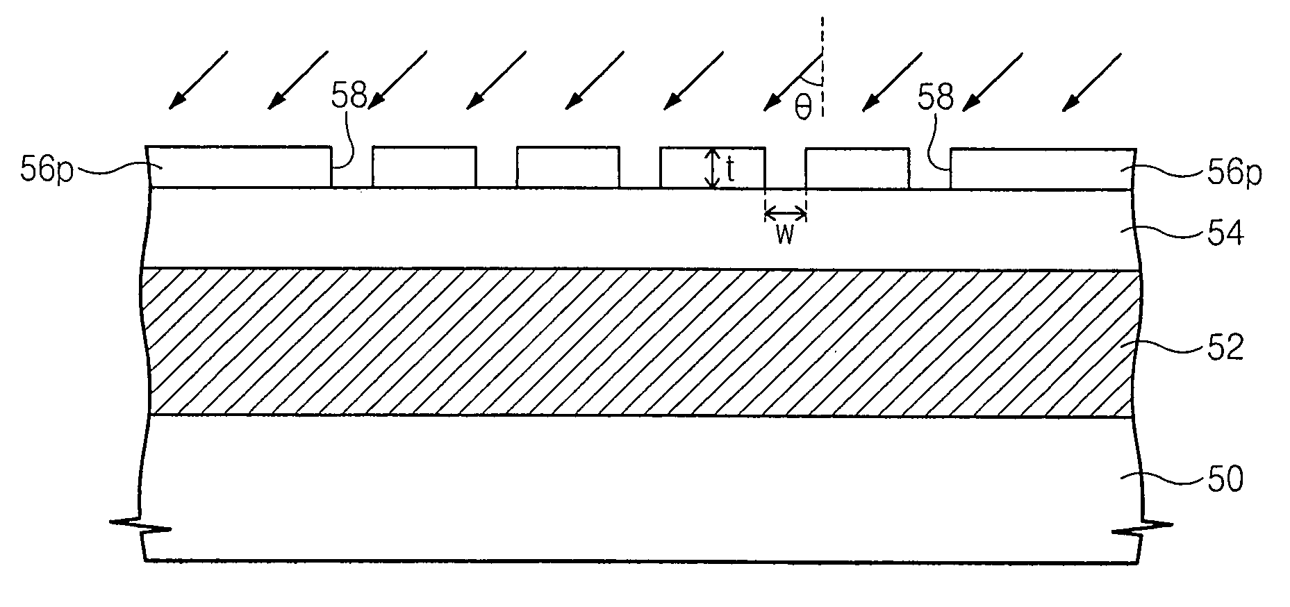
[0023] Referring to FIG. 5, a lower layer 52 is formed on a substrate 50. A lower photoresist layer 54 is formed on lower layer 52 and an upper photoresist layer 56 is formed on lower photoresist layer 54. Lower photoresist layer 54 typically comprises an anti-reflecting coating (ARC) film and may act as an etch-stop layer for upper photoresist layer 56. Lower photoresist layer 54 is typically formed to a thickness of at least 1 μm and submitted to a baking process performed at a temperature of 200° C. for 90 seconds. Upper photoresist layer 5...


PUM


Abstract

A method of forming a pattern for a semiconductor device is disclosed. According to the method, a lower photoresist layer is formed on a lower layer and an upper photoresist pattern including a silylated layer is formed on the lower photoresist layer. The upper photoresist pattern is used as a mask for etching the lower photoresist layer to thereby form a lower photoresist pattern. The upper and lower photoresist patterns are used as a mask for etching the lower layer beneath the lower photoresist pattern.

Description

BACKGROUND OF THE INVENTION [0001] 1. Field of the Invention [0002] The present invention relates generally to a method of fabricating a semiconductor device, and more particularly to a method of forming a pattern in a semiconductor device using a photolithographic process. [0003] A claim of priority is made to Korean Patent Application No. 2004-37811 filed on May 27, 2004, the disclosure of which is hereby incorporated by reference in its entirety. [0004] 2. Description of the Related Art [0005] Photolithographic processes are commonly used to create patterns in semiconductor devices. These patterns include, for example, trenches used to form circuits. In order to create smaller, higher performance semiconductor devices, methods for forming smaller patterns in the semiconductor devices are generally needed. [0006] Patterns are typically formed in semiconductor devices by forming a photoresist pattern on a semiconductor substrate using a photomask and then etching the semiconductor ...

Claims


Application Information

Patent Timeline
IPC IPC(8): G03F7/00G03F7/095G03F7/40H01L21/027H01L21/311H01L21/3213
CPCG03F7/095G03F7/405H01L21/32139H01L21/31144H01L21/0274
Inventor KOH, CHA-WONWOO, SANG-GYUNKIM, BYEONG-SOO
Owner SAMSUNG ELECTRONICS CO LTD
Why Eureka
Try Eureka