Photoresist polymer and photoresist composition containing the same

a technology of photoresist polymer and composition, which is applied in the direction of photosensitive materials, instruments, photomechanical equipment, etc., can solve the problems of not solving the above-described problems, the contact region of the storage electrode receives a relatively large amount of light, and the photoresist materials used in arf photolithography are more difficult to use than conventional photoresist materials, etc., to achieve good etching resistance and improve the profile of the storage electrode contact region

Inactive Publication Date: 2007-10-09
SK HYNIX INC
View PDF17 Cites 326 Cited by
  • Summary
  • Abstract
  • Description
  • Claims
  • Application Information

AI Technical Summary

Benefits of technology

[0007]Disclosed herein are photoresist polymers and photoresist compositions containing the same that can improve a profile of a storage electrode contact region which receives relatively large amount of light when a device isolation film pattern is formed and developed and wherein the photoresist polymers and compositions also provide good etching resistance.

Problems solved by technology

However, photoresist materials that have been used in ArF photolithography are more difficult to use than conventional photoresist materials.
However, a storage electrode contact region receives a relatively large amount of light due to the shape the device isolation film pattern around the electrode contact.
Although the amount of energy or exposure conditions of lens have been regulated in order to prevent the storage electrode contact region from being too thin, the above-described problems have not been solved.
In addition, there are problems in that the margins of DOF (Depth of Focus) and EL (Energy Latitude) become smaller as the pattern becomes smaller.
However, these problems cannot be solved by changing the exposure conditions.
Also, it is difficult to secure etching resistance because the thickness of the photoresist film becomes too thin to prevent pattern collapse.

Method used


Image

  • Photoresist polymer and photoresist composition containing the same
  • Photoresist polymer and photoresist composition containing the same
  • Photoresist polymer and photoresist composition containing the same

Examples


example 1

Preparation of Photoresist Polymer

[0048]To 25 ml of tetrahydrofuran in 100 ml of a round-shaped flask were added 5 g of 3-(trimethoxysilyl)propyl methacrylate, 4 g of t-butyl methacrylate, 3 g of methyl 5-norbornene-2-carboxylate and 3 g of maleic anhydride. Then, 0.13 g of AIBN (azobisisobutyronitrile) as a polymerization initiator was added to the resulting mixture, and reacted at 67° C. under a nitrogen atmosphere for 24 hours. Next, the resulting mixture was cooled at room temperature, and poured into a beaker including 500 ml of ethyl ether to precipitate the resulting mixture. Thereafter, the precipitate was filtered and dehydrated at room temperature, thereby obtaining poly(3-(trimethyoxysilyl)propyl methacrylate / t-butyl methacrylate / methyl 5-norbornene-2-carboxylate / maleic anhydride) having a molecular weight of 1,800 represented by formula 1a (yield: 50%).

example 2

Preparation of Photoresist Composition

[0049]To 50 g of methyl 3-methoxypropionate as an organic solvent were added 10 g of poly(3-(trimethyoxysilyl)propyl methacrylate / t-butyl methacrylate / methyl 5-norbornene-2-carboxylate / maleic anhydride) obtained from Example 1 and 0.1 g of triphenylsulfonium triflate as a photoacid generator. Then, the resulting mixture was filtered through a 0.10 μm filter to obtain a disclosed photoresist composition.

example 3

Formation of Photoresist Patterns

[0050]The photoresist composition obtained from Example 2 was spin-coated on a silicon wafer to form a photoresist film, and soft-baked at 90° C. for 90 seconds. After baking, the photoresist was exposed to light using a KrF laser exposer, and then post-baked at 110° C. for 90 seconds. The baked wafer was developed in 2.38 wt % TMAH aqueous solution for 40 seconds to obtain a L / S pattern of 120 nm.

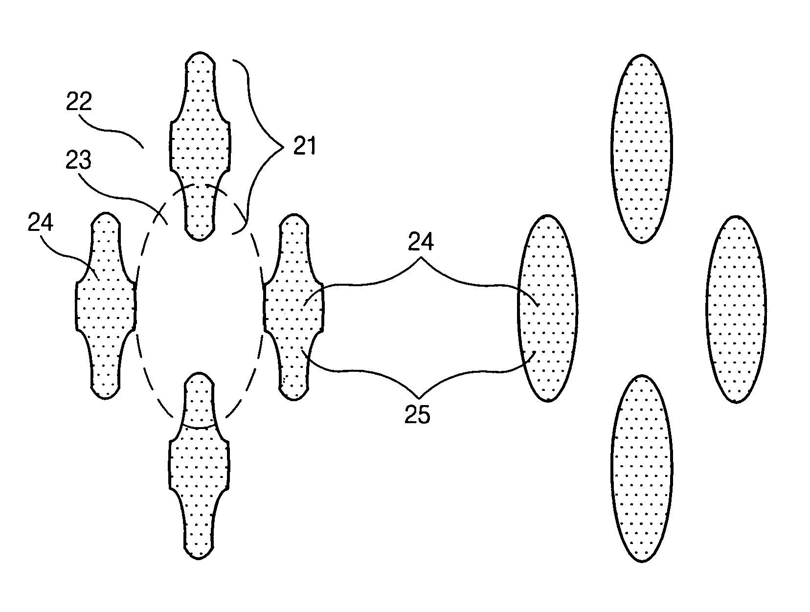
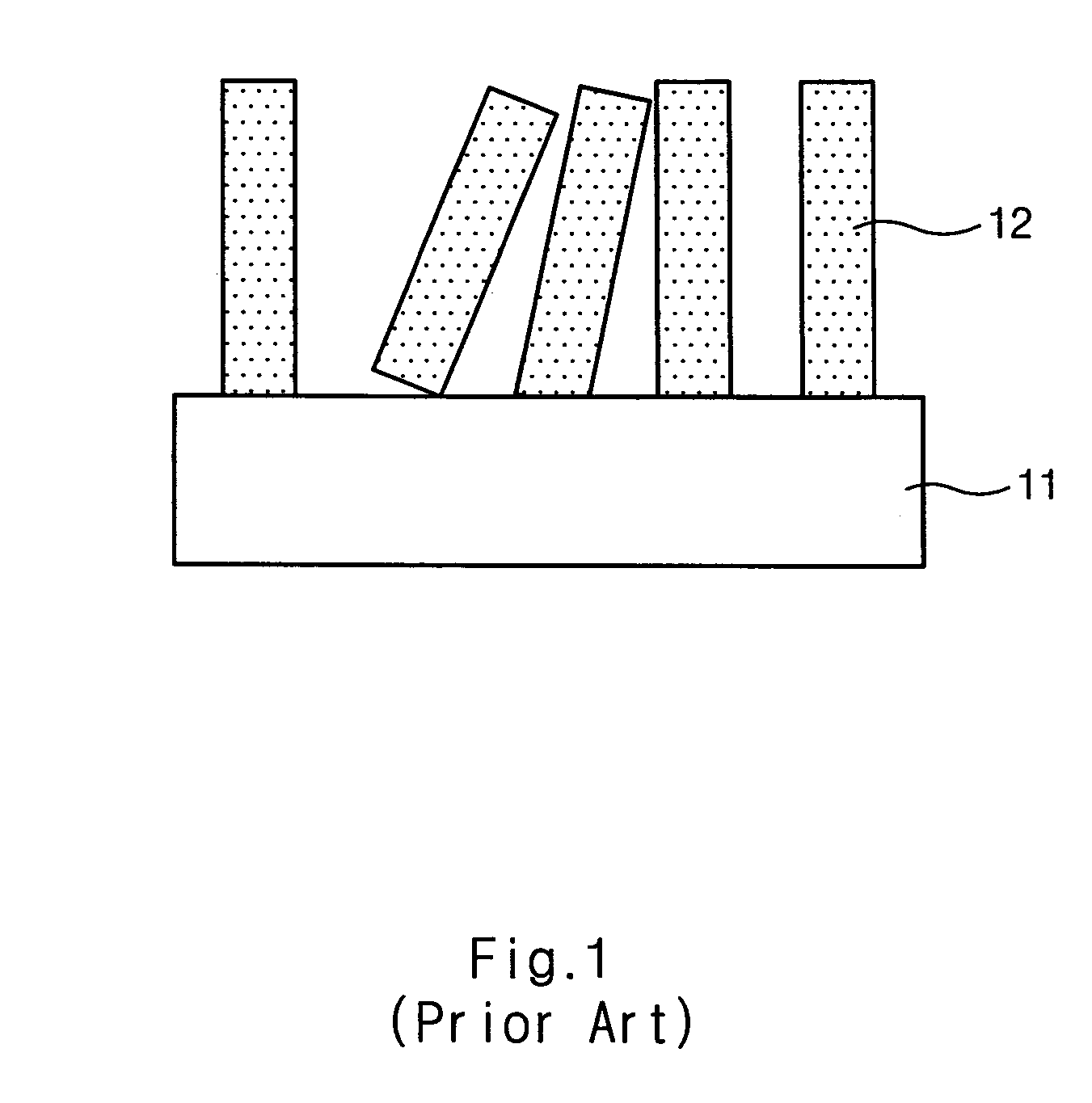
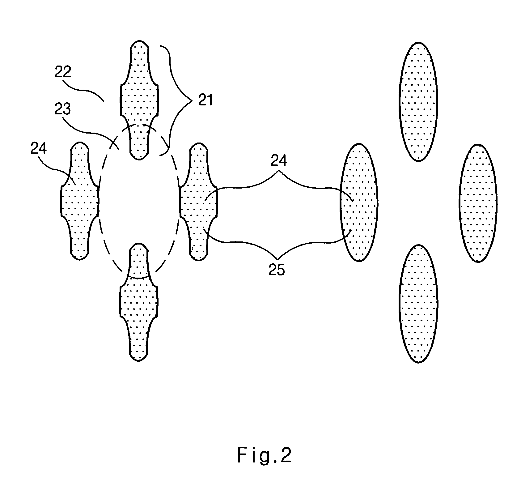
[0051]As described above, since the disclosed photoresist polymer is less sensitive to change in the amount of energy due to its higher active energy than that of a conventional photoresist polymer, a phenomenon that a pattern of a storage electrode contact region that receives a relatively large amount of light can be improved when a device isolation film pattern is formed, and pattern collapse caused by a high aspect ratio due to high etching resistance can be prevented. Therefore, the disclosed photoresist polymers and the photoresist compositions contai...


PUM

PropertyMeasurementUnit
temperatureaaaaaaaaaa
aspect ratioaaaaaaaaaa

Abstract

Photoresist polymers and photoresist compositions are disclosed. A photoresist polymer comprising a polymerization repeating unit represented by Formula I is less sensitive to change in the amount of energy due to its higher active energy than that of a conventional photoresist polymer. As a result, a phenomenon where the portion of the pattern for the storage electrode contact region that receives relatively large amount of light becomes too thin is avoided when the device isolation film pattern is formed, and wherein pattern collapse caused by a high aspect ratio due to high etching resistance is prevented or avoided.whereinR1–R10, a, b, c and d are as defined in the description.

Description

BACKGROUND[0001]1. Technical Field[0002]Photoresist polymers and photoresist compositions containing the same are disclosed that can avoid a phenomenon where a pattern of a storage electrode contact region that receives a relatively large amount of light becomes too thin when a device isolation film pattern is formed. The photoresist polymers and compositions can also prevent pattern collapse caused by a high aspect ratio by improving the etching resistance.[0003]2. Description of the Related Art[0004]As a manufacturing process of a semiconductor device becomes more complicated and the degree of integration is increased, methods for forming fine patterns are needed. Because it is difficult to obtain a fine pattern with conventional photolithography using KrF (248 nm), photolithography using a far-infrared light source such as ArF (193 nm) has been developed. However, photoresist materials that have been used in ArF photolithography are more difficult to use than conventional photore...

Claims


Application Information

Patent Timeline
Patent Type & Authority Patents(United States)
IPC IPC(8): G03F7/004
CPCC08F220/18C08F222/06C08F230/08C08F232/08G03F7/0758H01L21/0274G03F7/0395Y10S430/111Y10S430/106C08F230/085C08F220/1804G03F7/0392
Inventor SON, MIN SEOK
Owner SK HYNIX INC
Why Eureka
Try Eureka