
One component EUV photoresist

a photoresist and one-component technology, applied in the direction of photosensitive materials, auxiliaries/base layers of photosensitive materials, instruments, etc., can solve the problems of photoacid generators that will outgas under extreme ultraviolet, degradation of lenses used in extreme ultraviolet optics, and portion of photoacid generators of this type will outgas

Inactive Publication Date: 2006-02-28
INTEL CORP
View PDF6 Cites 319 Cited by
  • Summary
  • Abstract
  • Description
  • Claims
  • Application Information

AI Technical Summary

Benefits of technology

This patent is about improving the manufacturing process for semiconductor integrated circuits by using a new photoresist technology. The invention focuses on reducing outgassing of photoactive compounds and improving the resolution of the photoresist. By incorporating photoactive compounds into the polymer backbone of the photoresist, outgassing is reduced and the solubility switch is delayed during developing. This results in higher contrast and improved resolution. The use of photoactive compounds on the polymer backbone also reduces the amount of outgassing and prevents degradation of optical components. Overall, this technology allows for smaller feature sizes to be transferred by photolithographic processes.

Problems solved by technology

However, these photoacid generators will outgas under extreme ultraviolet irradiation under vacuum.
Outgassing may result in degradation of the lens used in the extreme ultraviolet optics due to photoresist fragment deposition related to outgassing.
However, the cation portion of the photoacid generators of this type will outgas after extreme ultraviolet irradiation.
However, the contrast achievable with such a structure limits the resolution of that photoresist.
As the acid diffusion length decreases, chemical amplification may be less efficient.
Since chemically amplified resists reach a point where they are no longer efficient, alternatives to chemical amplification are needed.

Method used


Image

  • One component EUV photoresist
  • One component EUV photoresist

Examples


Embodiment Construction

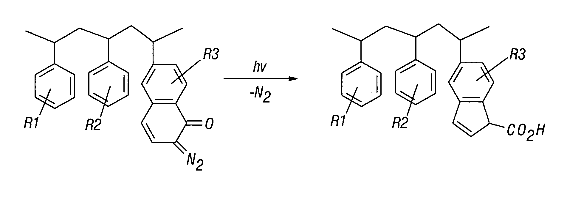
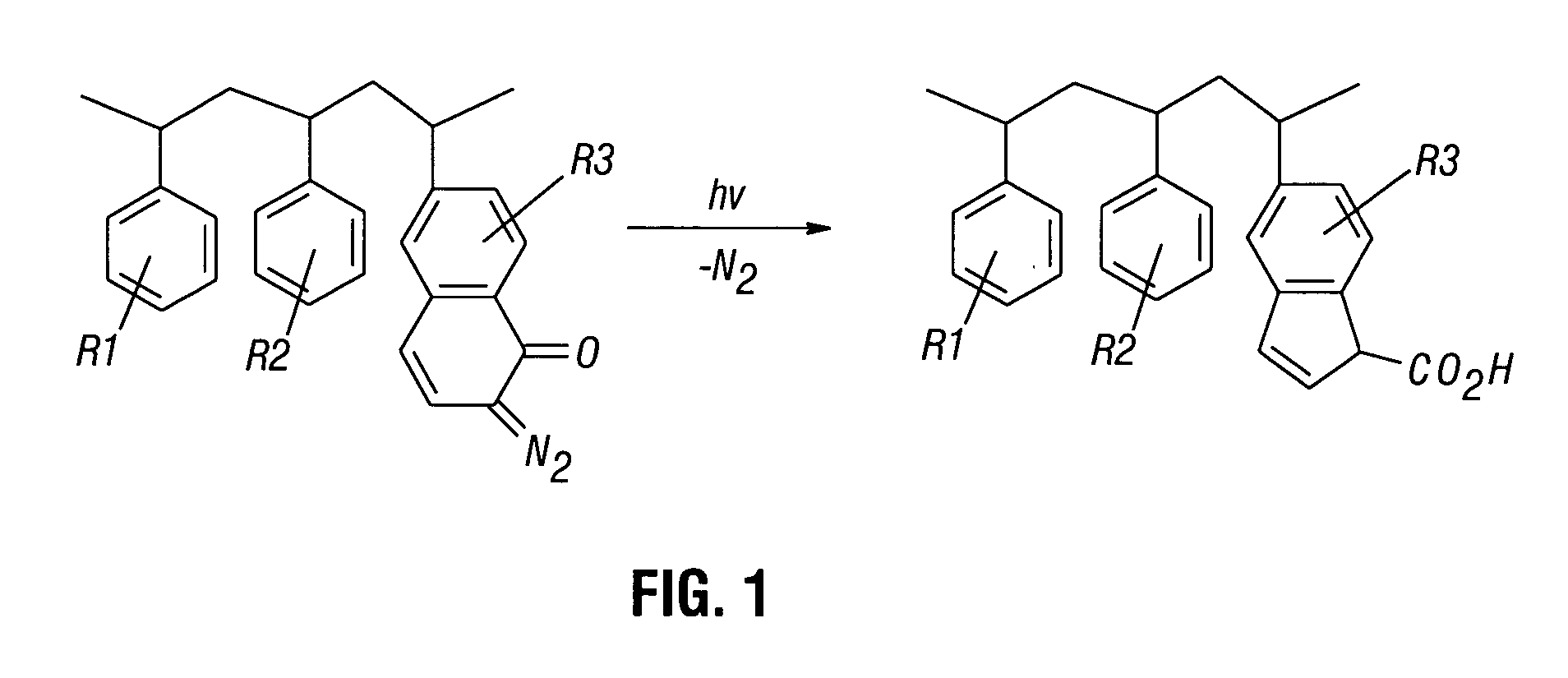
[0011]In one embodiment, by introducing photoactive compounds into the polymer backbone of the photoresist, outgassing of photo-reactive materials may be reduced. Photoactive compounds, such as diazonaphthoquinone (DNQ), may be incorporated on a polymer backbone via a conventional polymerization reaction, using initiators (such as AIBN, and phenyl peroxide, etc.). The photoactive compounds reduce the amount of outgassing of reactive materials. Since the diffusion of the photoacid generator is believed to be a primary source of line width roughness of chemically amplified photoresists, use of photoactive compounds on the polymer backbone may reduce line width roughness because large molecules will not diffuse over any significant distance.

[0012]As the photoactive compounds may be incorporated into the polymer backbone, a resist with high sensitivity and high contrast may be provided. Moreover, the breakdown of the photochemistry does not generate hydrocarbons (such as isobutene) as d...


PUM

PropertyMeasurementUnit
areaaaaaaaaaaa
solubilityaaaaaaaaaa
wavelengthsaaaaaaaaaa

Abstract

In one embodiment, a photoactive compound may be attached to a polymer backbone. This embodiment may be more resistant to the generation of reactive outgassing components and may exhibit better contrast.

Description

BACKGROUND[0001]This invention relates generally to the manufacture of semiconductor integrated circuits and, particularly, to photolithography processes for manufacturing such circuits.[0002]In the manufacture of semiconductor integrated circuits, a photoresist film is formed over a semiconductor wafer. The photoresist film may be irradiated so that some regions of the photoresist film are either harder or easier to dissolve in aquesios base developer. As a result, a pattern can be repeatedly transferred to the semiconductor wafer via the photoresist film. After developing, the photoresist film may be used as a mask for etching desired features in the underlying layers of the semiconductor wafer.[0003]Advances in photolithography techniques utilized to transfer patterns to photoresist have enabled increasingly smaller patterns to be transferred. This means that smaller integrated circuit features can be formed in integrated circuits. As a result, more elements can be put in a given...

Claims


Application Information

Patent Timeline
Patent Type & Authority Patents(United States)
IPC IPC(8): G03F7/023G03F7/30C08F8/30G03C1/76
CPCG03F7/023C08F8/30
Inventor YUEH, WANGCAO, HEIDI
Owner INTEL CORP
Learn More