Phase change memory device and method for forming the same

a phase change memory and memory device technology, applied in the field of semiconductor devices, can solve the problem of limiting the ability to reduce the size of the phase change memory device, and achieve the effect of reducing the operation curren

Active Publication Date: 2006-01-19
SAMSUNG ELECTRONICS CO LTD
View PDF8 Cites 75 Cited by
  • Summary
  • Abstract
  • Description
  • Claims
  • Application Information

AI Technical Summary

Benefits of technology

[0014] The present invention is directed to a phase change memory device which can minimize an operation current, and a method for forming the same.

Problems solved by technology

There is thus a limit in the ability to reduce the size of the phase change memory device.

Method used


Image

  • Phase change memory device and method for forming the same
  • Phase change memory device and method for forming the same
  • Phase change memory device and method for forming the same

Examples


first embodiment

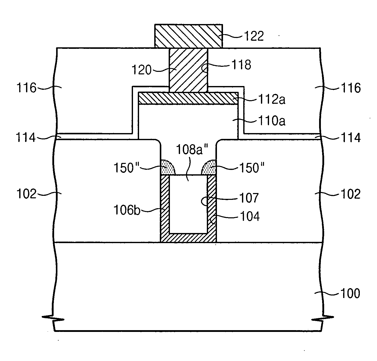
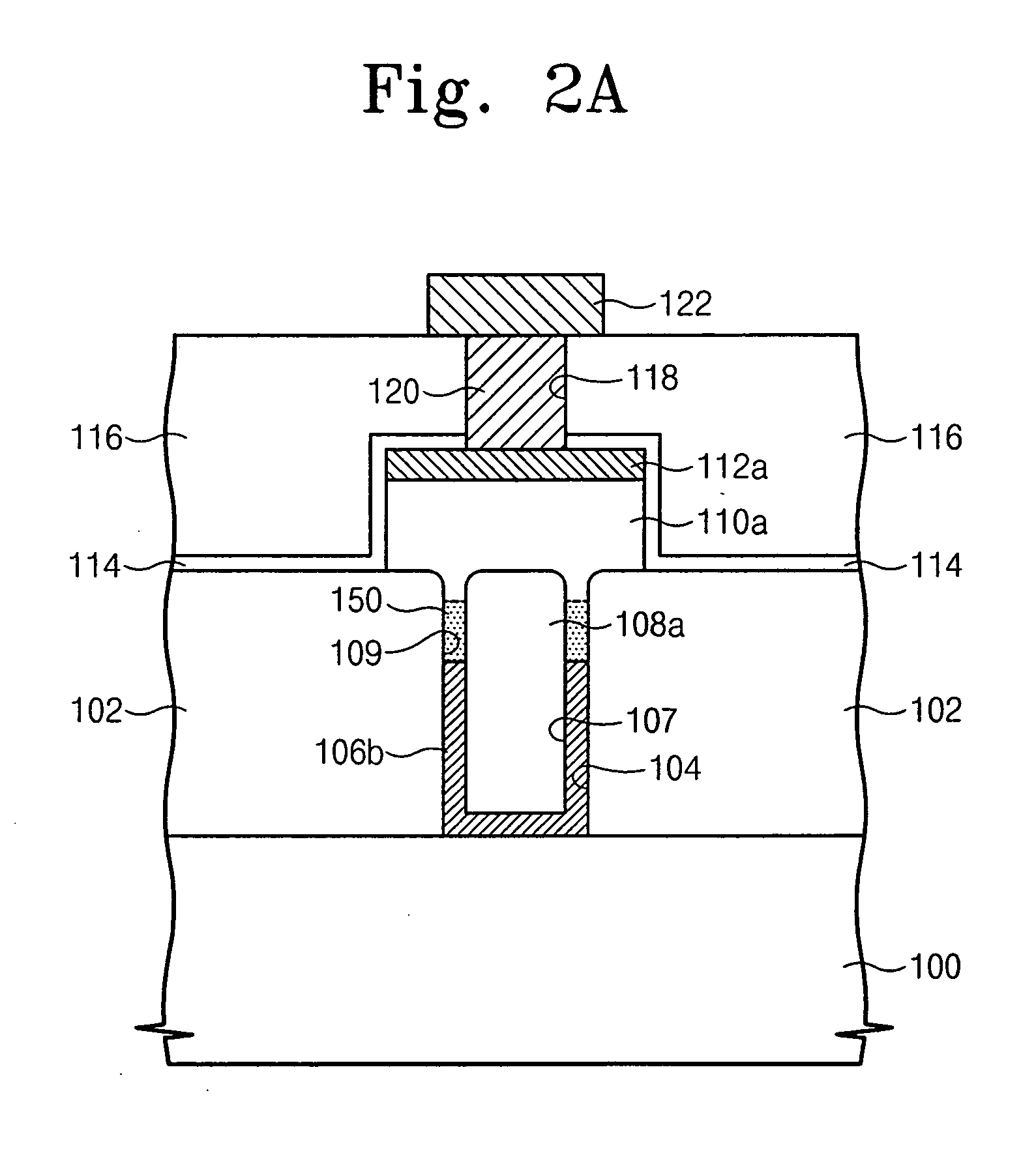
[0039]FIG. 2A is a cross-sectional diagram illustrating a phase change memory device in accordance with a first embodiment of the present invention.

[0040] As illustrated in FIG. 2A, a mold layer 102 made of an insulation film is disposed on a semiconductor substrate 100 (referred to as “substrate”). The mold layer 102 has an opening 104 exposing a predetermined region of the substrate 100. The opening 104 is formed in a hole shape.

[0041] A substantially cylindrical heating electrode 106b is disposed in the opening 104. The heating electrode 106b has its bottom portion contact the exposed substrate 100 and its sidewalls conformally disposed on the lower inner walls of the opening 104. The sidewalls of the heating electrode 106b are disposed along the circumference of the inner walls of the opening 104. Accordingly, the top surfaces of the sidewalls of the heating electrode 106b are lower than the top surface of the mold layer 102. A filling insulation pattern 108a is disposed at an...


PUM

PropertyMeasurementUnit
phaseaaaaaaaaaa
heightaaaaaaaaaa
conductiveaaaaaaaaaa

Abstract

A phase change memory device includes a mold layer disposed on a substrate, a heating electrode, a filling insulation pattern and a phase change material pattern. The heating electrode is disposed in an opening exposing the substrate through the mold layer. The heating electrode is formed in a substantially cylindrical shape, having its sidewalls conformally disposed on the lower inner walls of the opening. The filling insulation pattern fills an empty region surrounded by the sidewalls of the heating electrode. The phase change material pattern is disposed on the mold layer and downwardly extended to fill the empty part of the opening. The phase change material pattern contacts the top surfaces of the sidewalls of the heating electrode.

Description

CROSS-REFERENCE TO RELATED APPLICATIONS [0001] This U.S. non-provisional patent application claims priority under 35 U.S.C. § 119 of Korean Patent Application 2004-56000 filed on Jul. 19, 2004, the entire contents of which are hereby incorporated by reference. BACKGROUND OF THE INVENTION [0002] 1. Field of the Invention [0003] The present invention relates to a semiconductor device and a method for forming the same, and in particular, to a phase change memory device and a method for forming the same. [0004] 2. Description of the Related Art [0005] Recently, a phase change memory device has been suggested as a new semiconductor device. The phase change memory device has a nonvolatile property of maintaining stored data when power supply is stopped. A unit cell of the phase change memory device uses a phase change material as a data storing medium. The phase change material has two stable states (amorphous state and crystalline state) by a provided heat. A generally-known phase change...

Claims


Application Information

Patent Timeline
Patent Type & Authority Applications(United States)
IPC IPC(8): H01L47/00
CPCG11C2213/52Y10S438/90H01L45/06H01L45/1683H01L45/126H01L45/141H01L45/1233H10N70/8413H10N70/882H10N70/231H10N70/066H10N70/826
Inventor SONG, YOON-JONGLEE, SE-HOKIM, KI-NAMLEE, SU-YOUNPARK, JAE-HYUN
Owner SAMSUNG ELECTRONICS CO LTD
Why Eureka
Try Eureka