Organic electroluminescent display device and method for fabricating the same

a technology of electroluminescent display device and electroluminescent light, which is applied in the direction of discharge tube/lamp details, organic semiconductor device, discharge tube luminescnet screen, etc., can solve the problem of difficulty in forming optical films of different thicknesses

Active Publication Date: 2006-01-26
SAMSUNG DISPLAY CO LTD
View PDF2 Cites 81 Cited by
  • Summary
  • Abstract
  • Description
  • Claims
  • Application Information

AI Technical Summary

Problems solved by technology

However, it is very difficult to form optical films of different thicknesses by using different manufacturing processes for each color.

Method used


Image

  • Organic electroluminescent display device and method for fabricating the same
  • Organic electroluminescent display device and method for fabricating the same
  • Organic electroluminescent display device and method for fabricating the same

Examples


embodiment 1

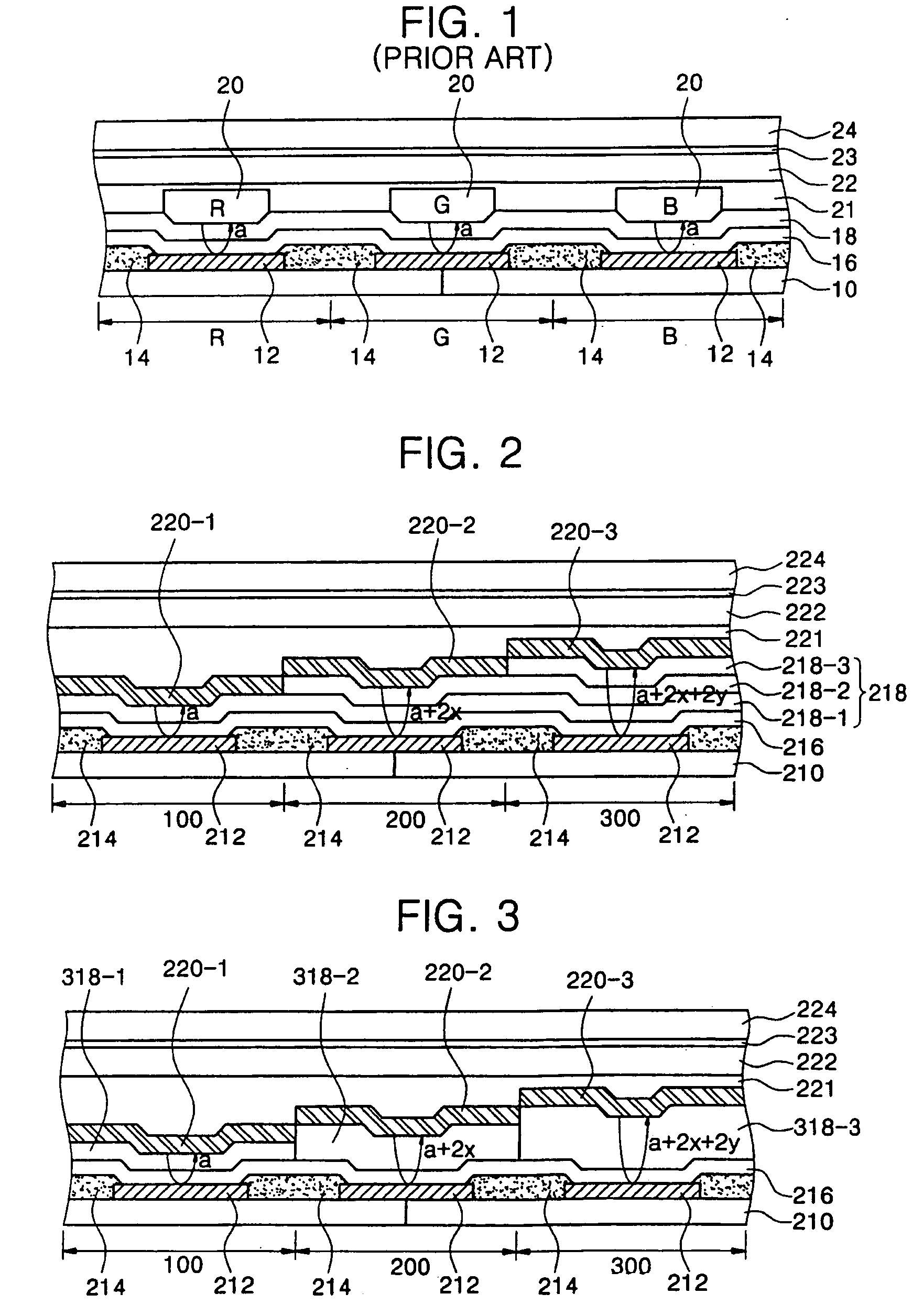
[0103] This embodiment describes a method for manufacturing an OELD device which has all of red, green and blue light emitting layers as an OELD device which is optimized in thickness of the hole injecting layer and the hole transporting layer.

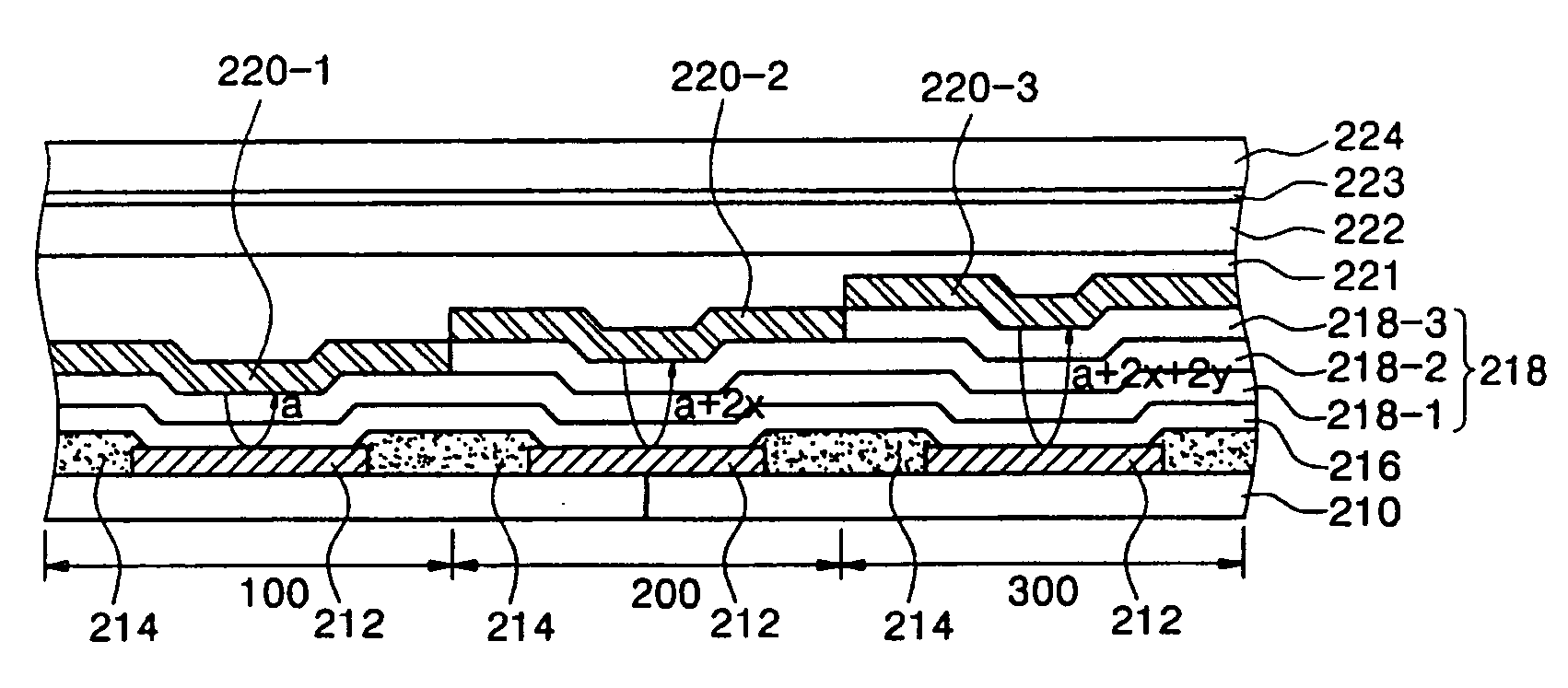
[0104] A substrate having a thin film transistor (TFT) is prepared, and a pixel electrode made of aluminum is formed at a thickness 1,000 ★ in the form of stripe. Here, the pixel electrode is formed to be electrically connected to source and drain electrodes of the TFT arranged on the lower substrate.

[0105] A pixel defining layer which defines regions on which red, green and blue light emitting layers are to be formed is formed on the pixel electrode using a silicon oxide material. Then, m-TDATA as a hole injecting material is deposited at a thickness of 1,000 ★ to form the hole injecting layer. NPB as a hole transporting material is deposited at a thickness of 400 ★ to form the hole transporting layer. Using a photo mask, NPB is additionall...

embodiment 2

[0110] This embodiment describes a method for manufacturing a flat panel display device which has two or more OELD devices to display through both sides.

[0111] A transparent substrate which has first and second display regions and a thin film transistor is prepared. A first OELD device is formed on the first display region of the substrate in the same way as Embodiment 1. A second OELD device which has layered structure of Table 2 below is formed on a surface corresponding to the surface on which the first OELD device is formed, thereby manufacturing the flat panel display device which can display through both sides. That is, the first OELD device is a front light emitting type which has a reflective pixel electrode and a transparent opposite electrode, whereas the second OELD device is a bottom light emitting type which has a transparent pixel electrode and a reflective opposite electrode.

TABLE 2Red light emitting regionGreen light emitting regionBlue light emitting regionPixel ...


PUM


Abstract

The present invention discloses organic electroluminescent display device and a method for fabricating the same, which includes: a first hole transporting layer formed in the first, second, and third pixel regions; a second hole transporting layer formed on a portion of the first hole transporting layer in the second and third pixel regions; a third hole transporting layer formed on a portion of the second hole transporting layer in the third pixel region. Light emitting layers are formed on each of the first, second, and third hole transporting layers. The thickness of the second hole transporting layer is approximately one-third (⅓) to two-thirds (⅔) of an optical wavelength difference between the first and second pixel regions, and the thickness of the third hole transporting layer is approximately one-third (⅓) to two-thirds (⅔) of an optical wavelength difference between the second and third pixel regions.

Description

CROSS-REFERENCE TO RELATED APPLICATION [0001] This application claims the benefit of Korean Patent Application No. 2004-57383, filed on Jul. 22, 2004, the disclosure of which is hereby incorporated in its entirety by reference herein. BACKGROUND OF THE INVENTION [0002] 1. Field of the Invention [0003] The present invention relates to an organic electroluminescent display device and a method of fabricating the same and, more particularly, to an organic electroluminescent display device having an optimum resonance structure. [0004] 2. Description of the Related Art [0005] An organic electroluminescent display (“OLED”) device having a thin film transistor (“TFT”) is a self light-emissive type display device, which is attracting public attention as a next generation display device because of its wide viewing angle, excellent contrast ratio, and fast response speed. [0006] The OLED device is classified as either an inorganic electroluminescent (EL) device or an organic EL device dependin...

Claims


Application Information

Patent Timeline
Patent Type & Authority Applications(United States)
IPC IPC(8): H05B33/00
CPCH01L27/3211H01L2251/558H01L51/5265H01L51/5048H10K59/35H10K50/14H10K50/156H10K50/852H10K2102/351H05B33/26H05B33/10
Inventor RYU, SEOUNG-YOON
Owner SAMSUNG DISPLAY CO LTD
Why Eureka
Try Eureka