

Optical system of a microlithographic projection exposure apparatus
- Summary
- Abstract
- Description
- Claims
- Application Information
AI Technical Summary
Benefits of technology
Problems solved by technology
Method used
Image

Examples
Embodiment Construction
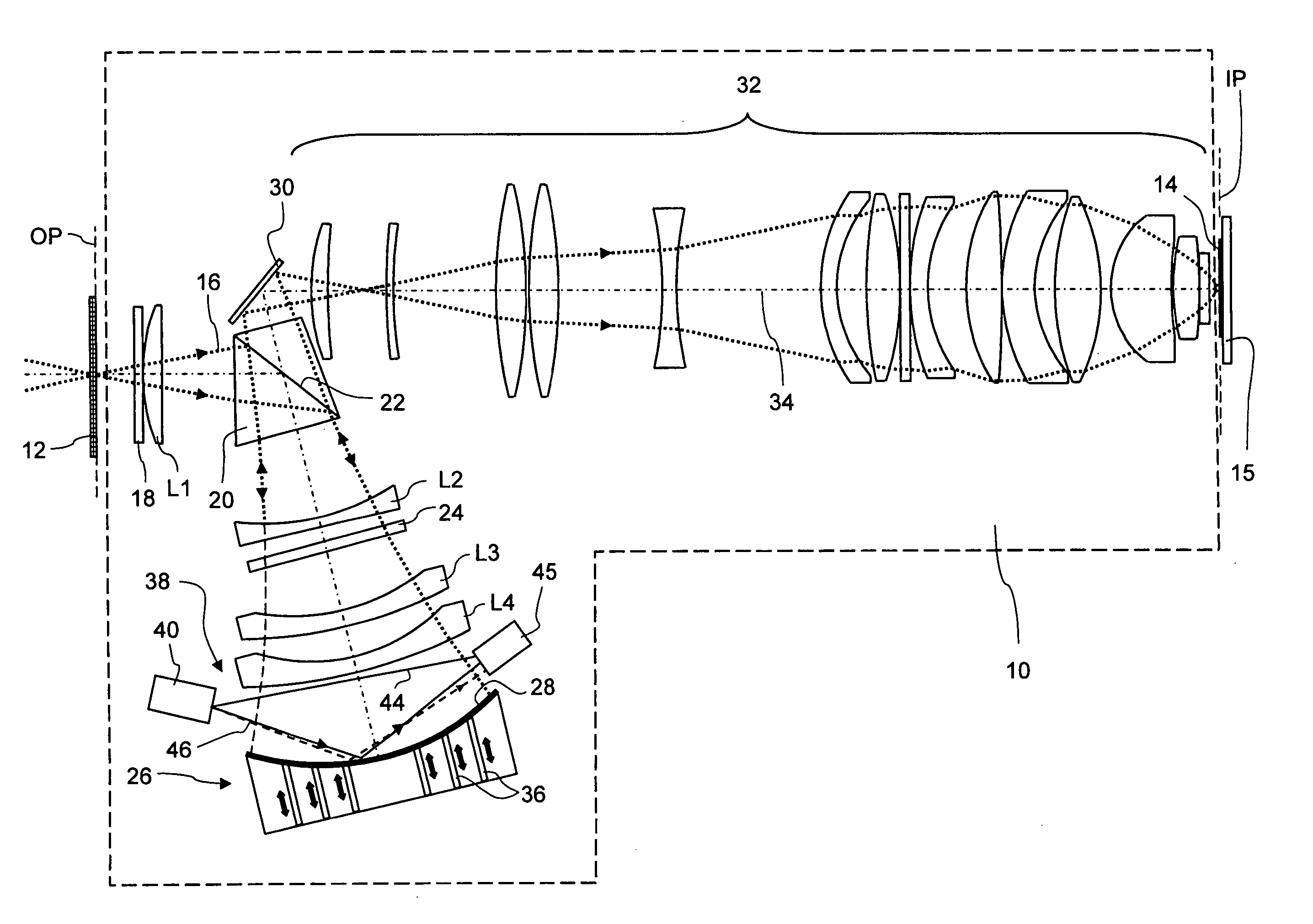
[0032]FIG. 1 represents a projection objective, denoted in its entirety by 10, of a microlithographic projection exposure apparatus in a simplified meridian section. The projection objective, which is also described in PCT / EP03 / 04015 filed by the applicant, is used to form a reduced image of structures, contained in a mask 12, onto a photosensitive layer 14 which consists of a photoresist and is applied on a substrate 15. The mask 12 is arranged in an object plane OP and the photosensitive layer 14 is arranged in an image plane IP of the projection objective 10.
[0033] After passing through the mask 12, the projection light 16 indicated by dots in FIG. 1, which is generated by an illumination system of the projection exposure apparatus and has a wavelength of 157 nm in the exemplary embodiment represented, travels through a plane-parallel plate 18 and a lens L1 into a beam-splitter cube 20. There, the projection light 16 is reflected at a polarization-selective beam-splitter layer 2...
PUM
 Abstract
Description
Claims
Application Information