

Surface emitting device and liquid crystal display device
- Summary
- Abstract
- Description
- Claims
- Application Information
AI Technical Summary
Benefits of technology
Problems solved by technology
Method used
Image

Examples
experimental example 1
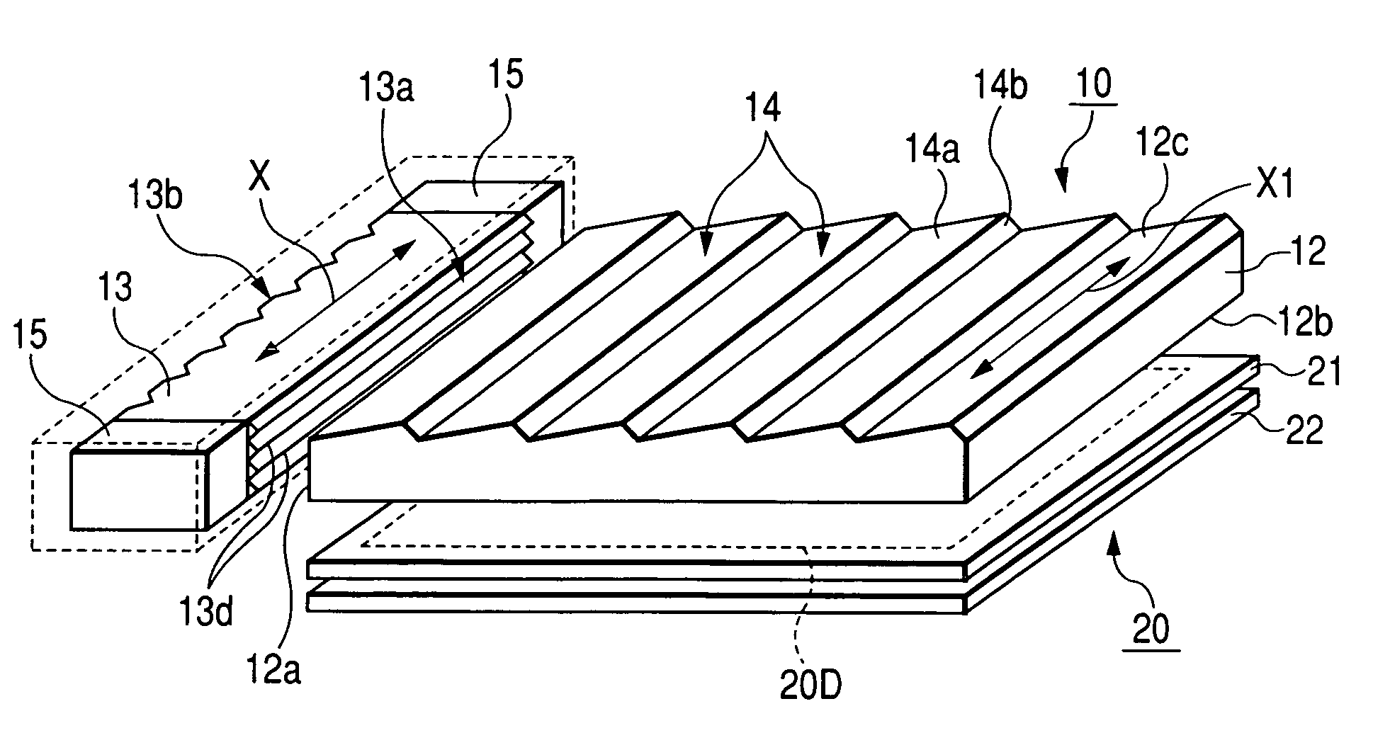
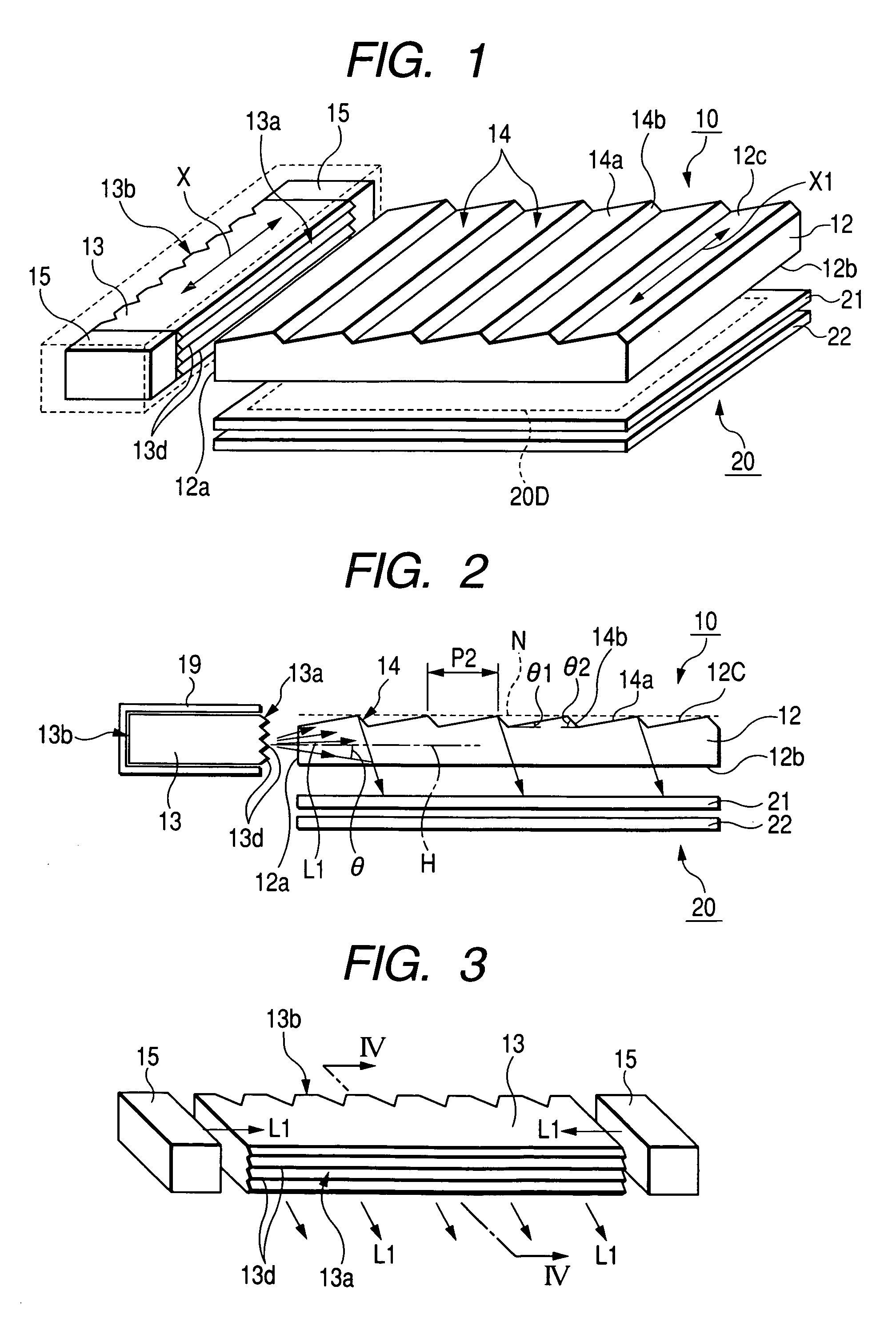
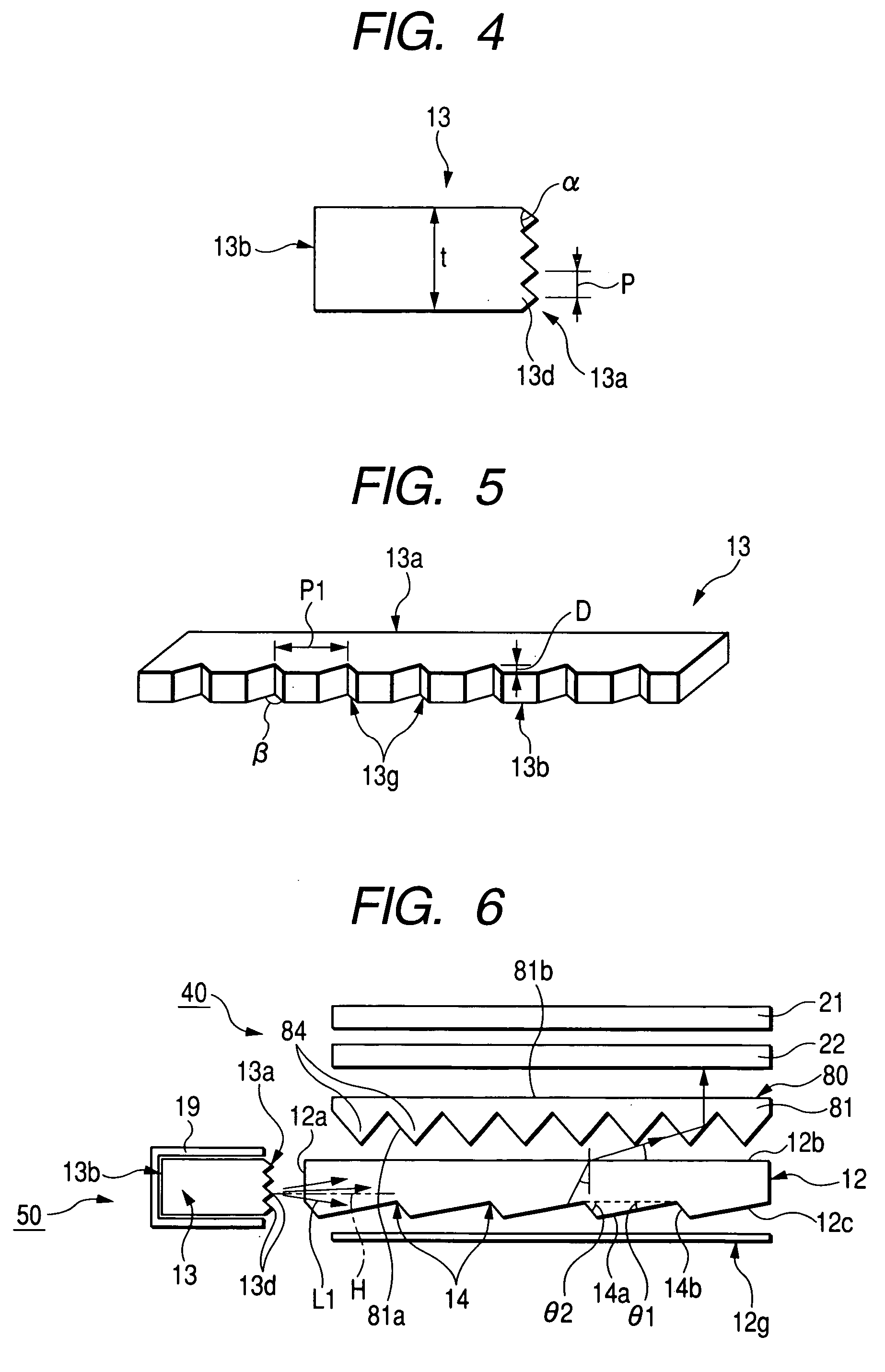
[0104] In the present experimental example, light emitted from the light emission surface 13a when the light-emitting elements 15 are turned on is received by a light-receiving unit BM-5A, and distribution of an emission angle of the light is measured, in a state where the apex angle of the projection 13d of the prism surface formed on the light emission surface 13a of the rod-shaped optical waveguide body 13 is set in the range of 45° to 120°, and the light source according to the embodiment shown in FIG. 1 or 6 (the rod-shaped optical waveguide body 13, the light-emitting elements 15 disposed at both sides of the rod-shaped optical waveguide body 13, and the case 19, made of Al, enclosing these components) is fabricated. The measured results are shown in FIG. 7.
[0105] For the purpose of comparison, the distribution of emission angles is also measured from the light source (a comparative example) having the same structure as that in the above-mentioned embodiment except that the l...
experimental example 2
[0108] Brightness inside the optical waveguide is measured using Risa-Color (manufactured by HI-LAND CO., LTD.) when the backlight (example) shown in FIG. 6 is manufactured by a combination of light source, the optical waveguide 12, the prism sheet 80, and the reflective plate 12g which are fabricated in the experimental example 1. The measured results are shown in FIGS. 8 to 10. In this case, when measuring the distribution of brightness, the inner surface of the optical waveguide is divided into twenty-five regions in plan view, and the brightness of a central point of each region is measured.
[0109] For the purpose of comparison, brightness inside the optical waveguide is measured in the same method as described above, when the backlight (comparative example) is manufactured by a combination of the light source and the optical waveguide 12 of the comparative example, which are fabricated in the experimental example 1. The measured results are shown in FIG. 11.
[0110] Furthermore,...
experimental example 3
[0121] The light source and the optical waveguide 12 according to this example fabricated in the experiment example 1 are combined to form the front light as shown in FIG. 1 (example).
[0122] Further, for the purpose of comparison, the light source and the optical waveguide 12 according to a comparative example fabricated in the experiment example 1 are combined to form the front light (comparative example).
[0123] The fabricated front light is disposed on the viewing side of the reflective liquid crystal unit 20 as shown in FIG. 1 to form a liquid crystal display device. Brightness and contrast (CR) of the display surface are measured when the front light is turned on. The measured results are shown in Table 1 and FIGS. 16 and 17.
TABLE 1Measured brightness and contrast of front lightLightemissionsurfaceof rod-shapedBrightness ofopticalBrightness of white displayblack displayContrastwaveguideApexAverageCentralBrightnessAverageCentralAverageCenterbodyanglebrightnessbrightnessunifor...
PUM
 Abstract
Description
Claims
Application Information