SERS-active structures having nanoscale dimensions
a technology of active structures and nanoscales, applied in the field of surface enhanced raman spectroscopy, can solve the problems of inability to produce such active structures, and inability to manufacture such active structures
- Summary
- Abstract
- Description
- Claims
- Application Information
AI Technical Summary
Benefits of technology
Problems solved by technology
Method used
Image

Examples
Embodiment Construction
[0028] The present invention, in a number of embodiments, includes SERS-active structures including features having nanoscale dimensions, methods for forming SERS-active structures, methods for forming a plurality of SERS-active structures, and methods for performing SERS using SERS-active structures.
[0029] The methods disclosed herein allow for the fabrication of SERS-active structures including nanoscale features having well controlled size, shape, location, and orientation, which allows for improved enhancement of the Raman scattered signal intensity relative to previous SERS-active structures.
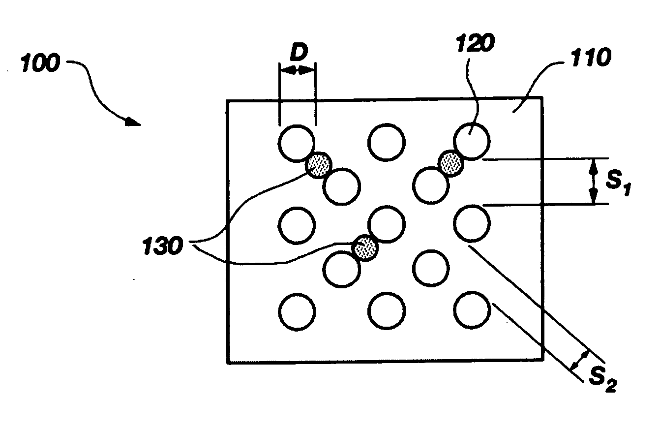
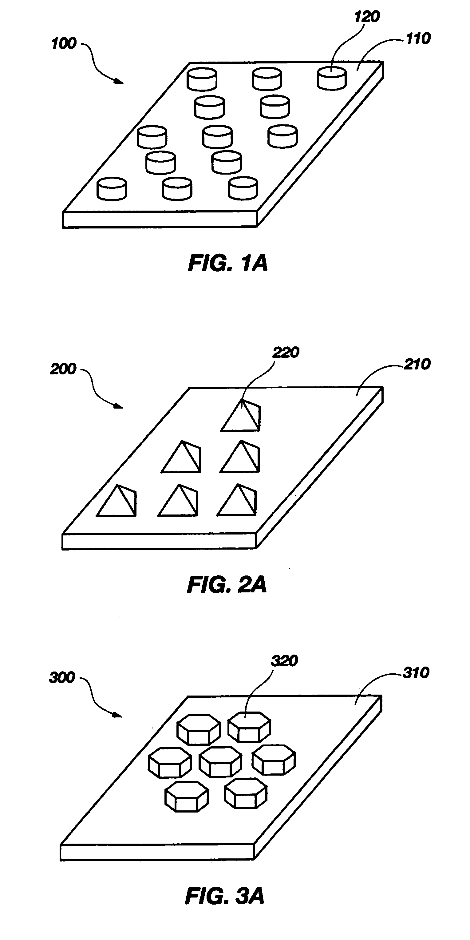
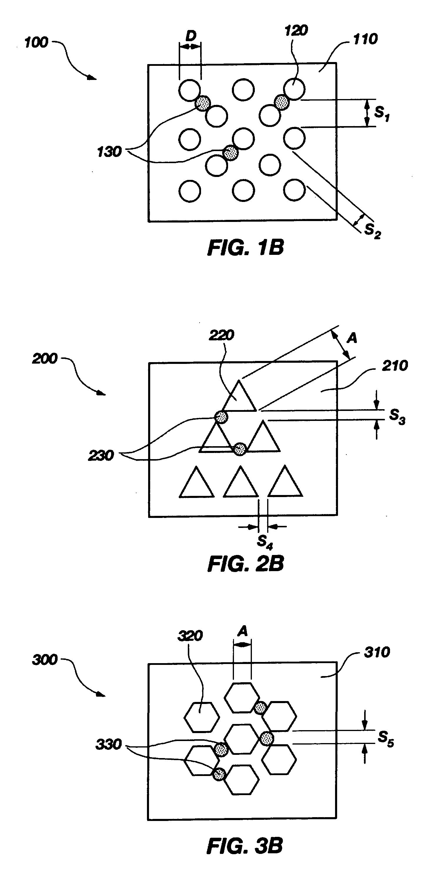
[0030] An exemplary SERS-active structure 100 is shown in FIGS. 1A-1B that may include a substrate 110 and an array of features 120 disposed at predetermined positions on a surface of the substrate 110. The substrate 110 may be formed from, for example, silicon, other semiconductor materials, ceramics, plastics, metals, or any other suitable material. Each feature 120 may be formed from a...
PUM
 Abstract
Description
Claims
Application Information
 - R&D Engineer
- R&D Manager
- IP Professional
- Industry Leading Data Capabilities
- Powerful AI technology
- Patent DNA Extraction
Browse by: Latest US Patents, China's latest patents, Technical Efficacy Thesaurus, Application Domain, Technology Topic.
© 2024 PatSnap. All rights reserved.Legal|Privacy policy|Modern Slavery Act Transparency Statement|Sitemap