Method for manufacturing plasma display panels

a technology of plasma display panels and plasma, which is applied in the direction of tube/lamp screen manufacturing, discharge tube general techniques, discharge tube coating, etc., can solve the problems of thin film peeling, dust generation, and detrimental effect on the quality of the film being formed

Inactive Publication Date: 2006-03-30
PANASONIC CORP
View PDF16 Cites 15 Cited by
  • Summary
  • Abstract
  • Description
  • Claims
  • Application Information

AI Technical Summary

Problems solved by technology

The thickened film then peels off into the deposition equipment, generating dust.
If such dust is present inside the deposition equipment, the dust may become embedded in the film during deposition or mix with the film material, having a detrimental effect on the quality of the film being formed.
Accordingly, there is a detrimental effect on the image display.

Method used


Image

  • Method for manufacturing plasma display panels
  • Method for manufacturing plasma display panels
  • Method for manufacturing plasma display panels

Examples


Embodiment Construction

)

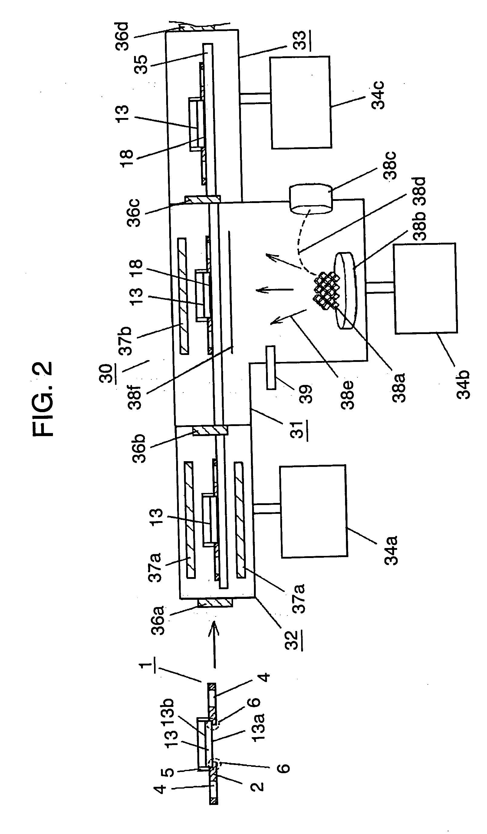
[0021] A PDP manufacturing method in accordance with a preferred embodiment of the present invention is described below with reference to drawings.

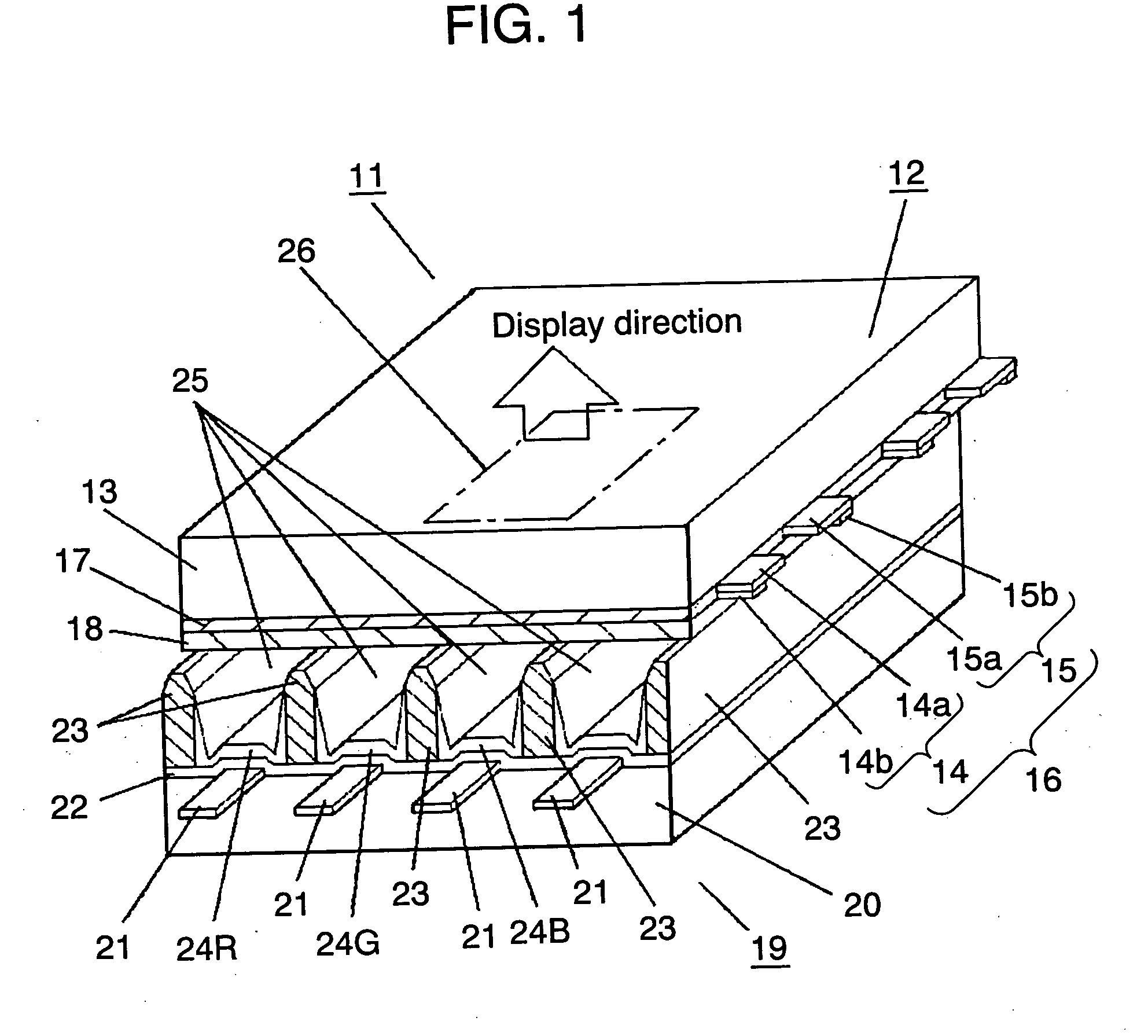
[0022] First, an example of a PDP structure is described. FIG. 1 is a sectional perspective view illustrating a schematic structure of the PDP made using the PDP manufacturing method in the preferred embodiment of the present invention.

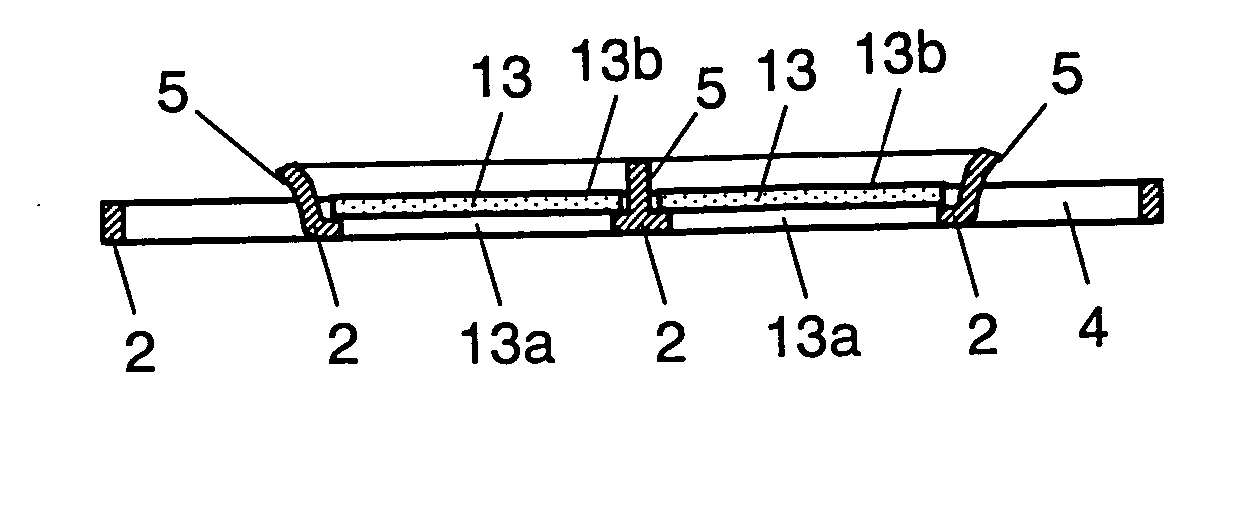
[0023] Front board 12 of PDP 11 has scanning display electrode 16, consisting of scan electrode 14 and sustain electrode 15; dielectric layer 17 covering this display electrode 16; and protective layer 18, typically made of MgO, further covering dielectric layer 17, on one main face at the front side of transparent insulating substrate 13, typically made of glass. Scan electrode 14 and sustain electrode 15 are configured by laminating bus electrodes 14b and 15b, made of a metal such as Ag, on transparent electrodes 14a and 15a so as to reduce electrical resistance.

[0024] Rear plate 19 at the back side h...


PUM

PropertyMeasurementUnit
heightaaaaaaaaaa
heightaaaaaaaaaa
pressureaaaaaaaaaa

Abstract

A method of manufacturing plasma display panels using a substrate holder for deposition on a substrate of the plasma display panel. The substrate holder is configured with plural frames, and the substrate of the plasma display panel is held by its periphery with at least one of these frames. A frame holding the substrate has a protrusion extending to a non-deposition face of the substrate held in such a way as to surround the substrate. Since the protrusion acts as a blocking sheet, attachment of a deposition material passing through an opening on the substrate holder and reaching onto the non-deposition face of the substrate is suppressed.

Description

TECHNICAL FIELD [0001] The present invention relates to methods of manufacturing plasma display panels (PDPs), a thin and light display device with a large screen, and more particularly to deposition on a substrate of the plasma display panel. The present invention also relates to substrate holders of the plasma display panels used during deposition. BACKGROUND ART [0002] In the PDP manufacture, for example, an electrode is formed on a substrate at the image display side. Then, a dielectric layer covering the electrode and a magnesium oxide (MgO) film covering the dielectric layer as a protective layer are formed. [0003] The electron-beam evaporation method is a widely used method for forming the protective layer, since it can form a relatively good quality MgO film at high deposition speeds (cf. “2001 FPD Technology Outlook”, Electronic Journal, Oct. 25, 2000, pp 598-600). [0004] With respect to deposition of the MgO film on the PDP substrate, the substrate is held with a substrate...

Claims


Application Information

Patent Timeline
Patent Type & Authority Applications(United States)
IPC IPC(8): B05D5/06B05D5/12C23C14/50H01J9/20H01J11/10H01L21/687
CPCC23C14/50H01J9/20H01J11/10Y02T50/67H01L21/68735H01L21/68778H01J2209/012Y02T50/60
Inventor SHINOZAKI, JUNTAKASE, MICHIHIKOFURUKAWA, HIROYUKI
Owner PANASONIC CORP
Why Eureka
Try Eureka