Multi display device and method of controlling the same

a multi-display and display panel technology, applied in static indicating devices, cathode-ray tube indicators, instruments, etc., can solve the problems of increasing the volume of an application device (e.g., mobile phone) and power consumption, and increasing the cost of common drive circuits. , to achieve the effect of preventing an increase in current consumption and reducing the occurrence of ghost images

Inactive Publication Date: 2006-04-27
SAMSUNG ELECTRONICS CO LTD
View PDF3 Cites 9 Cited by
  • Summary
  • Abstract
  • Description
  • Claims
  • Application Information

AI Technical Summary

Benefits of technology

[0018] Exemplary embodiments of the present invention provide a multi display device having a display control circuit for reducing the occurrence of a ghost image in at least one non-activated display panel due to a leakage current from an activated display panel, and for preventing an increase in current consumption due to the use of column lines that are shared in common by the activated display panel and the non-activated display panel.

Problems solved by technology

However, in the dual display device, the use of the two display panels may increase both cost and power consumption.
In such a case, noise between the display panels may be reduced; however, the use of the separate driving circuits for respective display panels may increase the volume of an application device (e.g., mobile phone) and power consumption.
Moreover, the common drive circuit is relatively expensive, resulting in increased costs.
Although the use of the common driver chip may result in lower device cost, noise and increased power consumption may occur due to an increase in parasitic capacitance of a wiring line.
Therefore, the ghost image due to the leakage current may appear on the sub display panel so that the image will appear distorted to the viewer.
Moreover, as described above, noise and increased power consumption may occur due to an increase in parasitic capacitance of a wiring line.

Method used


Image

  • Multi display device and method of controlling the same
  • Multi display device and method of controlling the same
  • Multi display device and method of controlling the same

Examples


Embodiment Construction

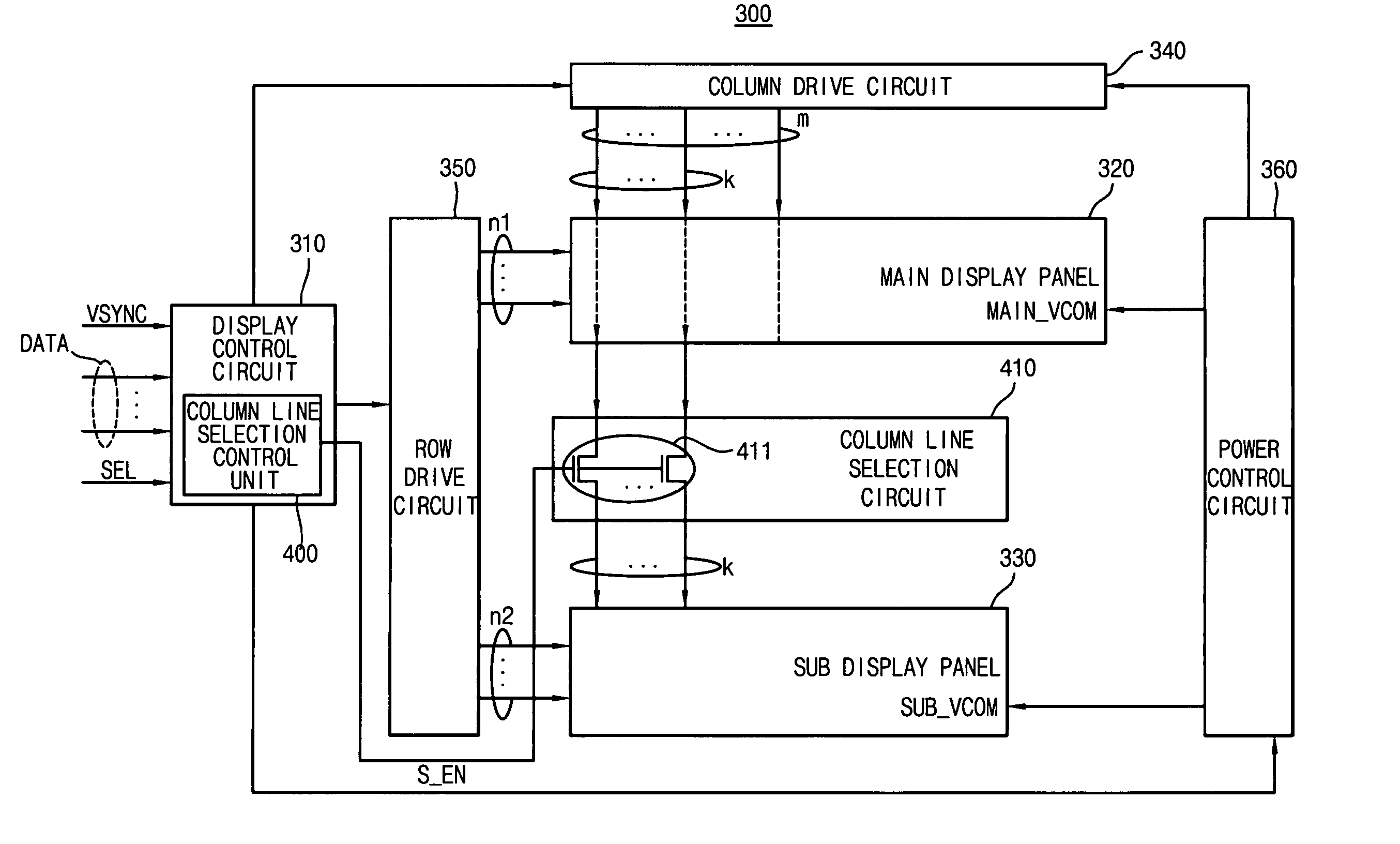
[0032] Hereinafter, exemplary embodiments of the present invention will be described in detail with reference to the accompanying drawings.

[0033] It will be understood that, although the terms first, second, etc. may be used herein to describe various elements, these elements should not be limited by these terms. These terms are only used to distinguish one element from another. For example, a first element could be termed a second element, and, similarly, a second element could be termed a first element, without departing from the scope of the present invention. As used herein, the term “and / or” includes any and all combinations of one or more of the associated listed items.

[0034] It will be understood that when an element is referred to as being “connected” or “coupled” to another element, it can be directly connected or coupled to the other element or intervening elements may be present. In contrast, when an element is referred to as being “directly connected” or “directly coup...


PUM


Abstract

A multi display device includes a row drive circuit, a column drive circuit and a column line selection circuit. The row drive circuit drives first row lines of a first display panel and second row lines of at least one second display panel. The column drive circuit drives first column lines of the first display panel and second column lines of the second display panel. The column line selection circuit controls a connection between the column drive circuit and one of the first column lines and the second column lines based on a column line selection signal.

Description

CROSS-REFERENCE TO RELATED APPLICATIONS [0001] This application claims priority to Korean Patent Application No. 2004-84220, filed on Oct. 21, 2004, the content of which is hereby incorporated by reference in its entirety. BACKGROUND OF THE INVENTION [0002] 1. Field of the Invention [0003] The present invention relates to a multi display device and a method of controlling the same. More particularly, the present invention relates to a multi display device that includes a drive circuit and a backlight unit shared in common by multiple display panels, which may prevent degradation in display quality such as the occurrence of a ghost image due to a leakage current drawn from an activated display panel. [0004] 2. Description of the Related Art [0005] A portable electronic device incorporating a display module may include a main display panel that displays a large amount of text and images and a sub display panel that displays a small amount of text and images. For example, in a mobile d...

Claims


Application Information

Patent Timeline
Patent Type & Authority Applications(United States)
IPC IPC(8): G09G5/00
CPCG09G3/20G09G3/3648G09G2300/0408G09G2310/0221G09G2310/0267G09G2310/0275G09G2320/0209G09G3/36
Inventor KANG, IM-SOOLEE, JAE-GOO
Owner SAMSUNG ELECTRONICS CO LTD
Why Eureka
Try Eureka